参数资料
| 型号: | AD5346BRUZ |
| 厂商: | Analog Devices Inc |
| 文件页数: | 10/24页 |
| 文件大小: | 0K |
| 描述: | IC DAC 8BIT OCTAL VOUT 38TSSOP |
| 产品培训模块: | Data Converter Fundamentals DAC Architectures |
| 标准包装: | 50 |
| 设置时间: | 6µs |
| 位数: | 8 |
| 数据接口: | 并联 |
| 转换器数目: | 8 |
| 电压电源: | 单电源 |
| 功率耗散(最大): | 8.3mW |
| 工作温度: | -40°C ~ 105°C |
| 安装类型: | 表面贴装 |
| 封装/外壳: | 38-TFSOP(0.173",4.40mm 宽) |
| 供应商设备封装: | 38-TSSOP |
| 包装: | 管件 |
| 输出数目和类型: | 8 电压,单极;8 电压,双极 |
| 采样率(每秒): | 167k |
AD5346/AD5347/AD5348
Rev. 0 | Page 18 of 24
The bias generator, the output amplifier, the resistor string, and
all other associated linear circuitry are all shut down when the
power-down mode is activated. However, the contents of the
registers are unaffected when in power-down. The time to exit
power-down is typically 2.5 s for VDD = 5 V and 5 s when VDD =
3 V. This is the time from a rising edge on the PD pin to when
the output voltage deviates from its power-down voltage. See
SUGGESTED DATA BUS FORMATS
In many applications, the GAIN and BUF pins are hardwired.
However, if more flexibility is required, they can be included in
a data bus. This enables the user to software program GAIN,
giving the option of doubling the resolution in the lower half of
the DAC range. In a bused system, GAIN and BUF may be
treated as data inputs because they are written to the device
during a write operation and take effect when LDAC is taken
low. This means that the reference buffers and the output
amplifier gain of multiple DAC devices can be controlled using
common GAIN and BUF lines. Note that GAIN and BUF are
not read back during an RD operation.
The AD5347 and AD5348 data bus must be at least 10 and 12
bits wide, respectively, and are best suited to a 16-bit data bus
system.
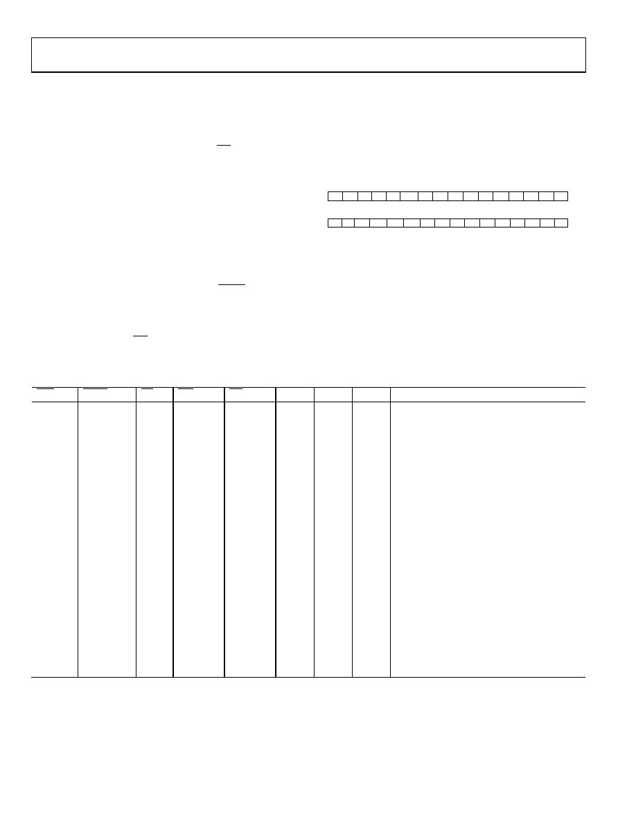
Examples of data formats for putting GAIN and BUF on a
16-bit data bus are shown in Figure 40. Note that any unused
bits above the actual DAC data may be used for GAIN and BUF.
03331-0-048
DB0
DB1
DB2
DB3
DB4
DB5
DB6
DB7
DB8
DB9
GAIN
X
BUF
X
X = UNUSED BIT
X
DB0
DB1
DB2
DB3
DB4
DB5
DB6
DB7
DB8
DB9
GAIN
X
BUF
DB11 DB10
AD5347
AD5348
Figure 40. AD5347/AD5348 Data Format for Word Load with
GAIN and BUF Data on 16-Bit Bus
Table 8. AD5346/AD5347/AD5348 Truth Table
CLR
LDAC
CS
WR
RD
A2
A1
A0
Function
1
X
No Data Transfer
1
X
1
X
No Data Transfer
0
X
Clear All Registers
1
0
→1
1
0
Load DAC A Input Register
1
0
→1
1
0
1
Load DAC B Input Register
1
0
→1
1
0
1
0
Load DAC C Input Register
1
0
→1
1
0
1
Load DAC D Input Register
1
0
→1
1
0
Load DAC E Input Register
1
0
→1
1
0
1
Load DAC F Input Register
1
0
→1
1
0
Load DAC G Input Register
1
0
→1
1
Load DAC H Input Register
1
X
0
1
→0
0
Read Back DAC Register A
1
X
0
1
→0
0
1
Read Back DAC Register B
1
X
0
1
→0
0
1
0
Read Back DAC Register C
1
X
0
1
→0
0
1
Read Back DAC Register D
1
X
0
1
→0
1
0
Read Back DAC Register E
1
X
0
1
→0
1
0
1
Read Back DAC Register F
1
X
0
1
1→0
1
0
Read Back DAC Register G
1
X
0
1
→0
1
Read Back DAC Register H
1
0
X
1
X
Update DAC Registers
X
0
X
Invalid Operation
X = Don’t Care
相关PDF资料 |
PDF描述 |
|---|---|
| VI-J5V-MY | CONVERTER MOD DC/DC 5.8V 50W |
| VI-J5T-MY | CONVERTER MOD DC/DC 6.5V 50W |
| LTC1450LCN#PBF | IC D/A CONV 12BIT R-R PAR 24-DIP |
| VI-J5R-MY | CONVERTER MOD DC/DC 7.5V 50W |
| LTC1450LCN | IC D/A CONV 12BIT R-R PAR 24-DIP |
相关代理商/技术参数 |
参数描述 |
|---|---|
| AD5346BRUZ | 制造商:Analog Devices 功能描述:IC 8BIT DAC SERIAL I/F OCTAL 5346 |
| AD5346BRUZ-REEL7 | 功能描述:IC DAC 8BIT OCTAL VOUT 38TSSOP 制造商:analog devices inc. 系列:- 包装:带卷(TR) 零件状态:在售 位数:8 数模转换器数:8 建立时间:8μs 输出类型:Voltage - Buffered 差分输出:无 数据接口:并联 参考类型:外部 电压 - 电源,模拟:2.5 V ~ 5.5 V 电压 - 电源,数字:2.5 V ~ 5.5 V INL/DNL(LSB):±0.15,±0.02 架构:电阻串 DAC 工作温度:-40°C ~ 105°C 封装/外壳:38-TFSOP(0.173",4.40mm 宽) 供应商器件封装:38-TSSOP 标准包装:1,000 |
| AD5346BRUZRUZ | 制造商:Analog Devices 功能描述:DAC,AD5346B 8bit 8us octal TSSOP |
| AD5347 | 制造商:AD 制造商全称:Analog Devices 功能描述:2.5 V to 5.5 V, Parallel Interface 2.5 V to 5.5 V, Parallel Interface |
| AD5347BCP | 制造商:Analog Devices 功能描述:DAC 8-CH Resistor-String 10-bit 40-Pin LFCSP EP 制造商:Analog Devices 功能描述:10BIT DAC SERIAL I/F OCTAL 5347 |
发布紧急采购,3分钟左右您将得到回复。