参数资料
| 型号: | AD5346BRUZ |
| 厂商: | Analog Devices Inc |
| 文件页数: | 13/24页 |
| 文件大小: | 0K |
| 描述: | IC DAC 8BIT OCTAL VOUT 38TSSOP |
| 产品培训模块: | Data Converter Fundamentals DAC Architectures |
| 标准包装: | 50 |
| 设置时间: | 6µs |
| 位数: | 8 |
| 数据接口: | 并联 |
| 转换器数目: | 8 |
| 电压电源: | 单电源 |
| 功率耗散(最大): | 8.3mW |
| 工作温度: | -40°C ~ 105°C |
| 安装类型: | 表面贴装 |
| 封装/外壳: | 38-TFSOP(0.173",4.40mm 宽) |
| 供应商设备封装: | 38-TSSOP |
| 包装: | 管件 |
| 输出数目和类型: | 8 电压,单极;8 电压,双极 |
| 采样率(每秒): | 167k |
AD5346/AD5347/AD5348
Rev. 0 | Page 20 of 24
DECODING MULTIPLE AD5346/AD5347/AD5348s
The CS pin on these devices can be used in applications to
decode a number of DACs. In this application, all DACs in the
system receive the same data and WR pulses, but only the CS to
one of the DACs will be active at any one time, so data will only
be written to the DAC whose CS is low.
The 74HC139 is used as a 2-line to 4-line decoder to address
any of the DACs in the system. To prevent timing errors from
occurring, the enable input should be brought to its inactive
state while the coded address inputs are changing state.
Figure 44 shows a diagram of a typical setup for decoding
multiple devices in a system. Once data has been written
sequentially to all DACs in a system, all the DACs can be
updated simultaneously using a common LDAC line. A com-
mon CLR line can also be used to reset all DAC outputs to 0 V.
ENABLE
CODED
ADDRESS
1G
1A
1B
VDD
VCC
74HC139
DGND
1Y0
1Y1
1Y2
1Y3
A0
A1
A2
WR
LDAC
CLR
DATA
INPUTS
DATA
INPUTS
DATA
INPUTS
DATA
INPUTS
DAT
A
BUS
A0
A1
A2
WR
LD AC
CLR
CS
A0
A1
A2
WR
LD AC
CLR
CS
AD5346/AD5347
/AD5348
A0
A1
A2
WR
LD AC
CLR
CS
A0
A1
A2
WR
LD AC
CLR
CS
AD5346/AD5347
/AD5348
AD5346/AD5347
/AD5348
AD5346/AD5347
/AD5348
03331-
0-
027
Figure 44. Decoding Multiple DAC Devices
AD5346/AD5347/AD5348 AS DIGITALLY
PROGRAMMABLE WINDOW DETECTORS
A digitally programmable upper/lower limit detector using two
of the DACs in the AD5346/AD5347/AD5348 is shown in
Figure 45. Any pair of DACs in the device may be used, but for
simplicity the description refers to DACs A and B.
The upper and lower limits for the test are loaded to DACs A
and B which, in turn, set the limits on the CMP04. If a signal at
the VIN input is not within the programmed window, an LED
indicates the fail condition.
5V
GND
VREFAB
VDD
VIN
FAIL
PASS
1k
1k
PASS/
FAIL
1/6 74HC05
1/2
CMP04
VREF
0.1
F
10
F
VOUTB
VOUTA
AD5346/AD5347/
AD5348
03331-
0-
028
Figure 45. Programmable Window Detector
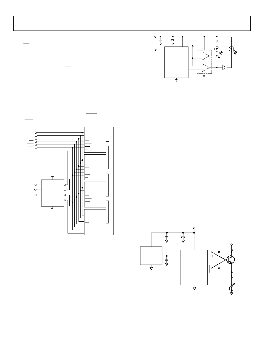
PROGRAMMABLE CURRENT SOURCE
Figure 46 shows the AD5346/AD5347/AD5348 used as the
control element of a programmable current source. In this
example, the full-scale current is set to 1 mA. The output
voltage from the DAC is applied across the current setting
resistor of 4.7 k in series with the 470 adjustment
potentiometer, which gives an adjustment of about ±5%.
Suitable transistors to place in the feedback loop of the ampli-
fier include the BC107 and the 2N3904, which enable the
current source to operate from a minimum VSOURCE of 6 V. The
operating range is determined by the operating characteristics
of the transistor. Suitable amplifiers include the AD820 and the
OP295, both having rail-to-rail operation on their outputs. The
current for any digital input code and resistor value can be
calculated as follows:
mA
R
D
V
G
I
N
REF
)
2
(
×
=
where:
G is the gain of the buffer amplifier (1 or 2).
D is the digital input code.
N is the DAC resolution (8, 10, or 12 bits).
R is the sum of the resistor plus adjustment potentiometer in k.
VDD = 5V
5V
LOAD
VSOURCE
EXT
REF
GND
VOUT
4.7k
470
*ONLY ONE CHANNEL OF VREF AND VOUT SHOWN
0.1
F
0.1
F
10
F
VIN
GND
AD5346/AD5347/
AD5348
VDD
VREF*VOUT*
03331-0-029
Figure 46. Programmable Current Source
相关PDF资料 |
PDF描述 |
|---|---|
| VI-J5V-MY | CONVERTER MOD DC/DC 5.8V 50W |
| VI-J5T-MY | CONVERTER MOD DC/DC 6.5V 50W |
| LTC1450LCN#PBF | IC D/A CONV 12BIT R-R PAR 24-DIP |
| VI-J5R-MY | CONVERTER MOD DC/DC 7.5V 50W |
| LTC1450LCN | IC D/A CONV 12BIT R-R PAR 24-DIP |
相关代理商/技术参数 |
参数描述 |
|---|---|
| AD5346BRUZ | 制造商:Analog Devices 功能描述:IC 8BIT DAC SERIAL I/F OCTAL 5346 |
| AD5346BRUZ-REEL7 | 功能描述:IC DAC 8BIT OCTAL VOUT 38TSSOP 制造商:analog devices inc. 系列:- 包装:带卷(TR) 零件状态:在售 位数:8 数模转换器数:8 建立时间:8μs 输出类型:Voltage - Buffered 差分输出:无 数据接口:并联 参考类型:外部 电压 - 电源,模拟:2.5 V ~ 5.5 V 电压 - 电源,数字:2.5 V ~ 5.5 V INL/DNL(LSB):±0.15,±0.02 架构:电阻串 DAC 工作温度:-40°C ~ 105°C 封装/外壳:38-TFSOP(0.173",4.40mm 宽) 供应商器件封装:38-TSSOP 标准包装:1,000 |
| AD5346BRUZRUZ | 制造商:Analog Devices 功能描述:DAC,AD5346B 8bit 8us octal TSSOP |
| AD5347 | 制造商:AD 制造商全称:Analog Devices 功能描述:2.5 V to 5.5 V, Parallel Interface 2.5 V to 5.5 V, Parallel Interface |
| AD5347BCP | 制造商:Analog Devices 功能描述:DAC 8-CH Resistor-String 10-bit 40-Pin LFCSP EP 制造商:Analog Devices 功能描述:10BIT DAC SERIAL I/F OCTAL 5347 |
发布紧急采购,3分钟左右您将得到回复。