参数资料
| 型号: | AD5405YCPZ |
| 厂商: | Analog Devices Inc |
| 文件页数: | 11/25页 |
| 文件大小: | 0K |
| 描述: | IC DAC DUAL 12BIT MULT 40-LFCSP |
| 产品培训模块: | Data Converter Fundamentals DAC Architectures |
| 标准包装: | 1 |
| 设置时间: | 80ns |
| 位数: | 12 |
| 数据接口: | 并联 |
| 转换器数目: | 2 |
| 电压电源: | 单电源 |
| 功率耗散(最大): | 50µW |
| 工作温度: | -40°C ~ 125°C |
| 安装类型: | 表面贴装 |
| 封装/外壳: | 40-VFQFN 裸露焊盘,CSP |
| 供应商设备封装: | 40-LFCSP-VQ(6x6) |
| 包装: | 托盘 |
| 输出数目和类型: | 4 电流,单极;4 电流,双极 |
| 采样率(每秒): | 21.3M |
| 产品目录页面: | 782 (CN2011-ZH PDF) |
| 配用: | EVAL-AD5405EB-ND - BOARD EVAL FOR AD5405 |
AD5405
Rev. B | Page 18 of 24
PARALLEL INTERFACE
Data is loaded into the AD5405 in a 12-bit parallel word format.
Control lines CS and R/W allow data to be written to or read
from the DAC register. A write event takes place when CS and
R/W are brought low, data available on the data lines fills the
shift register, and the rising edge of CS latches the data and
transfers the latched data-word to the DAC register. The DAC
latches are not transparent; therefore, a write sequence must
consist of a falling and rising edge on CS to ensure that data is
loaded into the DAC register and that its analog equivalent is
reflected on the DAC output. A read event takes place when
R/W is held high and CS is brought low. Data is loaded from the
DAC register, goes back into the input register, and is output
onto the data line, where it can be read back to the controller for
verification or diagnostic purposes. The input and DAC
registers of these devices are not transparent; therefore, a falling
and rising edge of CS is required to load each data-word.
MICROPROCESSOR INTERFACING
ADSP-21xx-to-AD5405 Interface
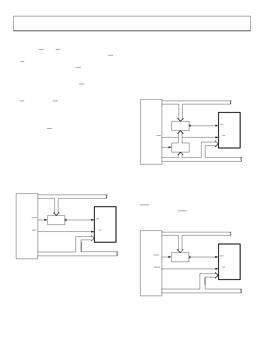
Figure 38 shows the AD5405 interfaced to the ADSP-21xx
series of DSPs as a memory-mapped device. A single wait state
may be necessary to interface the AD5405 to the ADSP-21xx,
depending on the clock speed of the DSP. The wait state can be
programmed via the data memory wait state control register of
the ADSP-21xx (see the ADSP-21xx family’s user manual for
details).
04463-
049
R/W
DB0 TO DB11
AD54051
ADDRESS
DECODER
CS
DATA 0 TO
DATA 23
ADDRESS BUS
ADDR0 TO
ADRR13
ADSP-21xx1
DATA BUS
DMS
WR
1ADDITIONAL PINS OMITTED FOR CLARITY.
Figure 38. ADSP21xx-to-AD5405 Interface
8xC51-to-AD5405 Interface
Figure 39 shows the interface between the AD5405 and the
8xC51 family of DSPs. To facilitate external data memory
access, the address latch enable (ALE) mode is enabled. The low
byte of the address is latched with this output pulse during
access to the external memory. AD0 to AD7 are the multiplexed
low order addresses and data bus; they require strong internal
pull-ups when emitting 1s. During access to external memory,
A8 to A15 are the high order address bytes. Because these ports
are open drained, they also require strong internal pull-ups
when emitting 1s.
04463-
051
R/W
DB0 TO DB11
AD54051
ADDRESS
DECODER
CS
AD0 TO AD7
ADDRESS BUS
A8 TO A15
80511
DATA BUS
WR
1ADDITIONAL PINS OMITTED FOR CLARITY.
8-BIT
LATCH
ALE
Figure 39. 8xC51-to-AD5405 Interface
ADSP-BF5xx-to-AD5405 Interface
Figure 40 shows a typical interface between the AD5405 and the
ADSP-BF5xx family of DSPs. The asynchronous memory write
cycle of the processor drives the digital inputs of the DAC. The
AMSx line is actually four memory select lines. Internal ADDR
lines are decoded into AMS3–0; these lines are then inserted as
chip selects. The rest of the interface is a standard handshaking
operation.
04463-
050
R/W
DB0 TO DB11
AD54051
ADDRESS
DECODER
CS
DATA 0 TO
DATA 23
ADDRESS BUS
ADDR1 TO
ADRR19
ADSP-BF5xx1
DATA BUS
AMSx
AWE
1ADDITIONAL PINS OMITTED FOR CLARITY.
Figure 40. ADSP-BF5xx-to-AD5405 Interface
相关PDF资料 |
PDF描述 |
|---|---|
| MS3452L32-63S | CONN RCPT 5POS BOX MNT W/SCKT |
| AD5316BRUZ | IC DAC 10BIT QUAD W/BUFF 16TSSOP |
| ICS843001CGILFT | IC CLK GEN FIBRE CH 8TSSOP |
| VI-2NX-MW-F1 | CONVERTER MOD DC/DC 5.2V 100W |
| VE-J53-MZ-F3 | CONVERTER MOD DC/DC 24V 25W |
相关代理商/技术参数 |
参数描述 |
|---|---|
| AD5405YCPZ-REEL | 功能描述:IC DAC DUAL 12BIT MULT 40LFCSP RoHS:是 类别:集成电路 (IC) >> 数据采集 - 数模转换器 系列:- 产品培训模块:LTC263x 12-, 10-, and 8-Bit VOUT DAC Family 特色产品:LTC2636 - Octal 12-/10-/8-Bit SPI VOUT DACs with 10ppm/°C Reference 标准包装:91 系列:- 设置时间:4µs 位数:10 数据接口:MICROWIRE?,串行,SPI? 转换器数目:8 电压电源:单电源 功率耗散(最大):2.7mW 工作温度:-40°C ~ 85°C 安装类型:表面贴装 封装/外壳:14-WFDFN 裸露焊盘 供应商设备封装:14-DFN-EP(4x3) 包装:管件 输出数目和类型:8 电压,单极 采样率(每秒):* |
| AD5405YCPZ-REEL7 | 功能描述:IC DAC DUAL 12BIT MULT 40LFCSP RoHS:是 类别:集成电路 (IC) >> 数据采集 - 数模转换器 系列:- 产品培训模块:LTC263x 12-, 10-, and 8-Bit VOUT DAC Family 特色产品:LTC2636 - Octal 12-/10-/8-Bit SPI VOUT DACs with 10ppm/°C Reference 标准包装:91 系列:- 设置时间:4µs 位数:10 数据接口:MICROWIRE?,串行,SPI? 转换器数目:8 电压电源:单电源 功率耗散(最大):2.7mW 工作温度:-40°C ~ 85°C 安装类型:表面贴装 封装/外壳:14-WFDFN 裸露焊盘 供应商设备封装:14-DFN-EP(4x3) 包装:管件 输出数目和类型:8 电压,单极 采样率(每秒):* |
| AD540J | 制造商:未知厂家 制造商全称:未知厂家 功能描述:Analog IC |
| AD540JH | 制造商:AD84/07 功能描述:Operational Amplifier, Single AMP, Bipolar/JFET, 8 Pin, Metal Can |
| AD540K | 制造商:未知厂家 制造商全称:未知厂家 功能描述:Analog IC |
发布紧急采购,3分钟左右您将得到回复。