参数资料
| 型号: | AD5405YCPZ |
| 厂商: | Analog Devices Inc |
| 文件页数: | 9/25页 |
| 文件大小: | 0K |
| 描述: | IC DAC DUAL 12BIT MULT 40-LFCSP |
| 产品培训模块: | Data Converter Fundamentals DAC Architectures |
| 标准包装: | 1 |
| 设置时间: | 80ns |
| 位数: | 12 |
| 数据接口: | 并联 |
| 转换器数目: | 2 |
| 电压电源: | 单电源 |
| 功率耗散(最大): | 50µW |
| 工作温度: | -40°C ~ 125°C |
| 安装类型: | 表面贴装 |
| 封装/外壳: | 40-VFQFN 裸露焊盘,CSP |
| 供应商设备封装: | 40-LFCSP-VQ(6x6) |
| 包装: | 托盘 |
| 输出数目和类型: | 4 电流,单极;4 电流,双极 |
| 采样率(每秒): | 21.3M |
| 产品目录页面: | 782 (CN2011-ZH PDF) |
| 配用: | EVAL-AD5405EB-ND - BOARD EVAL FOR AD5405 |
AD5405
Rev. B | Page 16 of 24
VOUT
VDD
GND
IOUT2A
IOUT1A
VREFA
RFBA
VDD
C1
12-BIT
DAC
R3
R2
R1
VIN
R1 = R2R3
R2 + R3
GAIN = R2 + R3
R2
04463-
011
NOTES
1. SIMILAR CONFIGURATION FOR DAC B.
Y BE REQUIRED
2. C1 PHASE COMPENSATION (1pF TO 2pF) MA
IF A1 IS A HIGH SPEED AMPLIFIER.
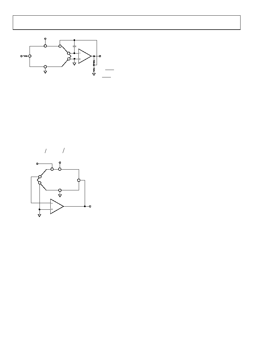
Figure 36. Increasing Gain of Current Output DAC
DIVIDER OR PROGRAMMABLE GAIN ELEMENT
Current-steering DACs are very flexible and lend themselves to
many applications. If this type of DAC is connected as the
feedback element of an op amp and RFBA is used as the input
resistor, as shown in Figure 37, the output voltage is inversely
proportional to the digital input fraction, D.
For D = 1 2n, the output voltage is
()n
IN
OUT
V
D
V
=
=
2
1
VOUT
VDD
GND
VIN
IOUT2A
REF
IOU
V
A
T1A
RFBA VDD
NOTES
1. ADDITIONAL PINS OMITTED FOR CLARITY.
04463-012
Figure 37. Current-Steering DAC Used as a Divider or
Programmable Gain Element
As D is reduced, the output voltage increases. For small
values of the digital fraction D, it is important to ensure that
the amplifier does not saturate and that the required accuracy is
met. For example, an 8-bit DAC driven with the binary code 0x10
(0001 0000)—that is, 16 decimal—in the circuit of Figure 37
should cause the output voltage to be 16 times VIN. However, if
th
weight in the range of 15.5/256 to 16.5/256 so that the possible
n error
or source in divider
ust be counterbalanced by an
the op amp through the DAC.
l
mperature coefficient specification. This parameter not
only affects the full-scale error, but also can affect the linearity
-
stem required to hold its overall
The primary requirement for the current-steering mode is an
e
een
he
This
ge in
to
.
kly.
e DAC has a linearity specification of ±0.5 LSB, D can have a
output voltage is in the range of 15.5 VIN to 16.5 VIN—a
of 3%, even though the DAC itself has a maximum error of 0.2%.
DAC leakage current is also a potential err
circuits. The leakage current m
opposite current supplied from
Because only a fraction, D, of the current into the VREF termina
is routed to the IOUT1 terminal, the output voltage changes as
follows:
Output Error Voltage Due to DAC Leakage = (Leakage × R)/D
where R is the DAC resistance at the VREF terminal.
For a DAC leakage current of 10 nA, R = 10 kΩ, and a gain (that
is, 1/D) of 16, the error voltage is 1.6 mV.
REFERENCE SELECTION
When selecting a reference for use with the AD54xx series of
current output DACs, pay attention to the reference’s output
voltage te
(INL and DNL) performance. The reference temperature coef-
ficient should be consistent with the system accuracy specifica
tions. For example, an 8-bit sy
specification to within 1 LSB over the temperature range 0°C to
50°C dictates that the maximum system drift with temperature
should be less than 78 ppm/°C. A 12-bit system with the same
temperature range to overall specification within 2 LSBs requires
a maximum drift of 10 ppm/°C. Choosing a precision reference
with low output temperature coefficient minimizes this error
source.
Table 7 lists some references available from Analog Devices that
are suitable for use with this range of current output DACs.
AMPLIFIER SELECTION
amplifier with low input bias currents and low input offset
voltage. Because of the code-dependent output resistance of th
DAC, the input offset voltage of an op amp is multiplied by the
variable gain of the circuit. A change in this noise gain betw
two adjacent digital fractions produces a step change in t
output voltage due to the amplifier’s input offset voltage.
output voltage change is superimposed on the desired chan
output between the two codes and gives rise to a differential
linearity error, which, if large enough, could cause the DAC
be nonmonotonic
The input bias current of an op amp also generates an offset at
the voltage output as a result of the bias current flowing in the
feedback resistor, RFB. Most op amps have input bias currents low
enough to prevent significant errors in 12-bit applications.
Common-mode rejection of the op amp is important in
voltage-switching circuits, because it produces a code-
dependent error at the voltage output of the circuit. Most
op amps have adequate common-mode rejection for use at
12-bit resolution.
Provided that the DAC switches are driven from true wideband,
low impedance sources (VIN and AGND), they settle quic
相关PDF资料 |
PDF描述 |
|---|---|
| MS3452L32-63S | CONN RCPT 5POS BOX MNT W/SCKT |
| AD5316BRUZ | IC DAC 10BIT QUAD W/BUFF 16TSSOP |
| ICS843001CGILFT | IC CLK GEN FIBRE CH 8TSSOP |
| VI-2NX-MW-F1 | CONVERTER MOD DC/DC 5.2V 100W |
| VE-J53-MZ-F3 | CONVERTER MOD DC/DC 24V 25W |
相关代理商/技术参数 |
参数描述 |
|---|---|
| AD5405YCPZ-REEL | 功能描述:IC DAC DUAL 12BIT MULT 40LFCSP RoHS:是 类别:集成电路 (IC) >> 数据采集 - 数模转换器 系列:- 产品培训模块:LTC263x 12-, 10-, and 8-Bit VOUT DAC Family 特色产品:LTC2636 - Octal 12-/10-/8-Bit SPI VOUT DACs with 10ppm/°C Reference 标准包装:91 系列:- 设置时间:4µs 位数:10 数据接口:MICROWIRE?,串行,SPI? 转换器数目:8 电压电源:单电源 功率耗散(最大):2.7mW 工作温度:-40°C ~ 85°C 安装类型:表面贴装 封装/外壳:14-WFDFN 裸露焊盘 供应商设备封装:14-DFN-EP(4x3) 包装:管件 输出数目和类型:8 电压,单极 采样率(每秒):* |
| AD5405YCPZ-REEL7 | 功能描述:IC DAC DUAL 12BIT MULT 40LFCSP RoHS:是 类别:集成电路 (IC) >> 数据采集 - 数模转换器 系列:- 产品培训模块:LTC263x 12-, 10-, and 8-Bit VOUT DAC Family 特色产品:LTC2636 - Octal 12-/10-/8-Bit SPI VOUT DACs with 10ppm/°C Reference 标准包装:91 系列:- 设置时间:4µs 位数:10 数据接口:MICROWIRE?,串行,SPI? 转换器数目:8 电压电源:单电源 功率耗散(最大):2.7mW 工作温度:-40°C ~ 85°C 安装类型:表面贴装 封装/外壳:14-WFDFN 裸露焊盘 供应商设备封装:14-DFN-EP(4x3) 包装:管件 输出数目和类型:8 电压,单极 采样率(每秒):* |
| AD540J | 制造商:未知厂家 制造商全称:未知厂家 功能描述:Analog IC |
| AD540JH | 制造商:AD84/07 功能描述:Operational Amplifier, Single AMP, Bipolar/JFET, 8 Pin, Metal Can |
| AD540K | 制造商:未知厂家 制造商全称:未知厂家 功能描述:Analog IC |
发布紧急采购,3分钟左右您将得到回复。