参数资料
| 型号: | AD5420AREZ |
| 厂商: | Analog Devices Inc |
| 文件页数: | 18/32页 |
| 文件大小: | 0K |
| 描述: | IC DAC 16BIT 1CH SER 24TSSOP |
| 产品培训模块: | Data Converter Fundamentals DAC Architectures Weigh Scale Introduction |
| 设计资源: | Simplified 16-Bit, 4 mA-to-20 mA Output Solution Using AD5420 (CN0098) |
| 标准包装: | 62 |
| 设置时间: | 10µs |
| 位数: | 16 |
| 数据接口: | DSP,MICROWIRE?,QSPI?,串行,SPI? |
| 转换器数目: | 1 |
| 电压电源: | 模拟和数字 |
| 功率耗散(最大): | 950mW |
| 工作温度: | -40°C ~ 85°C |
| 安装类型: | 表面贴装 |
| 封装/外壳: | 24-TSSOP(0.173",4.40mm)裸露焊盘 |
| 供应商设备封装: | 24-TSSOP 裸露焊盘 |
| 包装: | 管件 |
| 输出数目和类型: | 1 电流,单极 |
| 采样率(每秒): | * |
| 产品目录页面: | 782 (CN2011-ZH PDF) |
第1页第2页第3页第4页第5页第6页第7页第8页第9页第10页第11页第12页第13页第14页第15页第16页第17页当前第18页第19页第20页第21页第22页第23页第24页第25页第26页第27页第28页第29页第30页第31页第32页
Data Sheet
AD5410/AD5420
Rev. F | Page 25 of 32
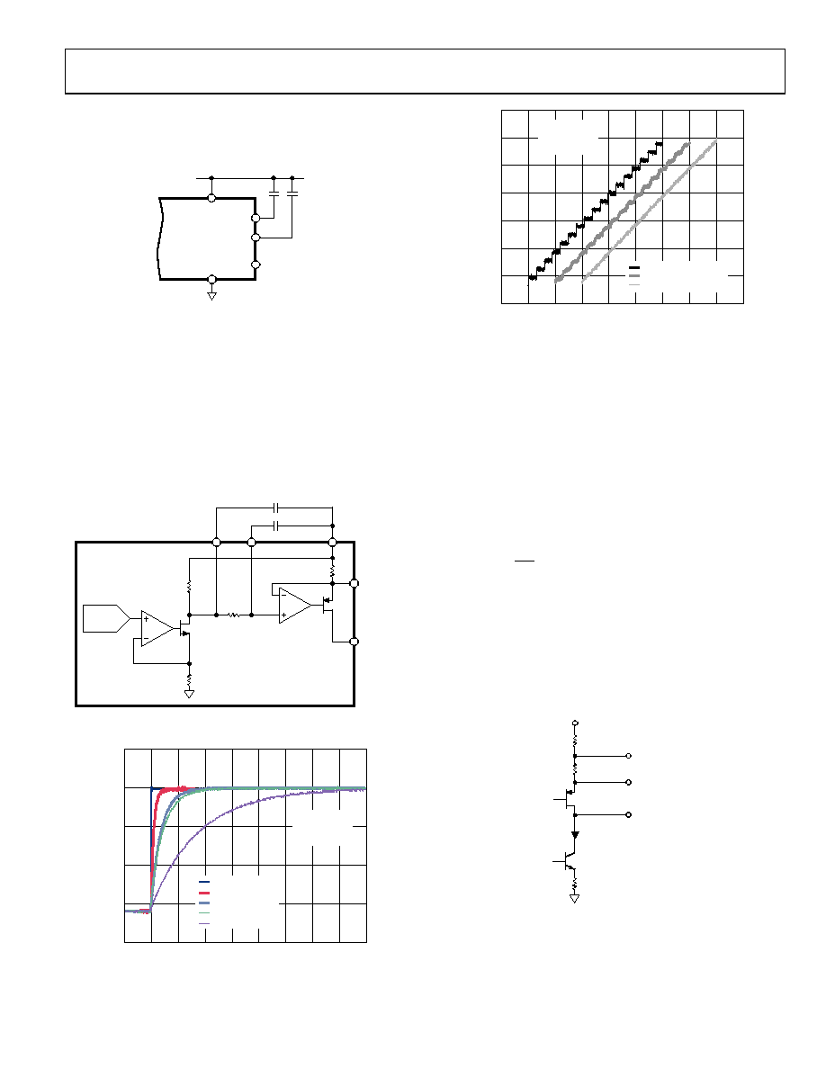
IOUT FILTERING CAPACITORS
Capacitors can be placed between CAP1 and AVDD, and CAP2
AD5410/
AD5420
CAP1
CAP2
07027-
037
AVDD
GND
C1
C2
IOUT
Figure 44. IOUT Filtering Capacitors
The capacitors form a filter on the current output circuitry, as
shown in Figure 45, reducing the bandwidth and the slew rate
of the output current. Figure 46 shows the effect the capacitors
have on the slew rate of the output current. To achieve significant
reductions in the rate of change, very large capacitor values are
required, which may not be suitable in some applications. In
this case, the digital slew rate control feature should be used.
The capacitors can be used in conjunction with the digital slew
rate control feature as a means of smoothing out the steps caused
by the digital code increments, as shown in Figure 47.
BOOST
CAP1
4k
40
DAC
12.5k
RSET
CAP2
IOUT
C1
C2
AVDD
07027-
038
Figure 45. IOUT Filter Circuitry
0
5
10
15
20
25
–0.5
0
0.5
1.0
1.5
2.0
2.5
3.0
3.5
4.0
O
UT
P
UT
CURRE
NT
(
mA)
TIME (ms)
NO CAPACITOR
10nF ON CAP1
10nF ON CAP2
47nF ON CAP1
47nF ON CAP2
07027-
142
TA = 25°C
AVDD = 24V
RLOAD = 300
Figure 46. Slew Controlled 4 mA to 20 mA Output Current Step Using
External Capacitors on the CAP1 and CAP2 Pins
6.1
6.2
6.3
6.4
6.5
6.6
6.7
6.8
–1
0
1
2
3
4
5
6
7
8
O
UT
P
UT
CURRE
NT
(
mA)
TIME (ms)
TA = 25°C
AVDD = 24V
RLOAD = 300
NO EXTERNAL CAPS
10nF ON CAP1
10nF ON CAP2
07027-
043
Figure 47. Smoothing Out the Steps Caused by the Digital Slew Rate Control
Feature
FEEDBACK/MONITORING OF OUTPUT CURRENT
For feedback or monitoring of the output current value, a sense
resistor can be placed in series with the IOUT output pin and the
voltage drop across it measured. As well as being an additional
component, the resistor increases the compliance voltage
required. An alternative method is to use a resistor that is
already in place. R3 is such a resistor and is internal to the
voltage between the R3SENSE and BOOST pins, the value of the
output current can be calculated as follows:
BIAS
R
OUT
I
R
V
I
=
3
(2)
where:
VR3 is the voltage drop across R3 measured between the R3SENSE
and BOOST pins.
IBIAS is a constant bias current flowing through R3 with a typical
value of 444 A.
R3 is the resistance value of resistor R3 with a typical value of 40 Ω.
AVDD
RMETAL
R3
40
444A
IBIAS
R3SENSE
IOUT
BOOST
07027-
050
Figure 48. Structure of Current Output Circuit
相关PDF资料 |
PDF描述 |
|---|---|
| VI-B0V-MY-F4 | CONVERTER MOD DC/DC 5.8V 50W |
| VE-26N-MW-F1 | CONVERTER MOD DC/DC 18.5V 100W |
| AD5453YRMZ-REEL7 | IC DAC 14BIT MULTIPLYING 8-MSOP |
| VI-B0V-MY-F3 | CONVERTER MOD DC/DC 5.8V 50W |
| VE-26L-MW-F4 | CONVERTER MOD DC/DC 28V 100W |
相关代理商/技术参数 |
参数描述 |
|---|---|
| AD5420AREZ-REEL7 | 功能描述:IC DAC 16BIT 1CH SER 24TSSOP RoHS:是 类别:集成电路 (IC) >> 数据采集 - 数模转换器 系列:- 标准包装:47 系列:- 设置时间:2µs 位数:14 数据接口:并联 转换器数目:1 电压电源:单电源 功率耗散(最大):55µW 工作温度:-40°C ~ 85°C 安装类型:表面贴装 封装/外壳:28-SSOP(0.209",5.30mm 宽) 供应商设备封装:28-SSOP 包装:管件 输出数目和类型:1 电流,单极;1 电流,双极 采样率(每秒):* |
| AD5420BCPZ | 制造商:AD 制造商全称:Analog Devices 功能描述:Single Channel, 16-Bit, Serial Input, Current Source DAC |
| AD5420BREZ | 制造商:Analog Devices 功能描述: |
| AD5421 | 制造商:AD 制造商全称:Analog Devices 功能描述:Low Power HART Modem |
| AD5421_11 | 制造商:AD 制造商全称:Analog Devices 功能描述:16-Bit, Serial Input, Loop-Powered, 4 mA to 20 mA DAC |
发布紧急采购,3分钟左右您将得到回复。