参数资料
| 型号: | AD5421CREZ |
| 厂商: | Analog Devices Inc |
| 文件页数: | 28/36页 |
| 文件大小: | 0K |
| 描述: | IC DAC 16BIT SPI/SRL 28TSSOP |
| 标准包装: | 50 |
| 设置时间: | 50µs |
| 位数: | 16 |
| 数据接口: | 串行,SPI? |
| 转换器数目: | 1 |
| 电压电源: | 单电源 |
| 功率耗散(最大): | 625mW |
| 工作温度: | -40°C ~ 105°C |
| 安装类型: | 表面贴装 |
| 封装/外壳: | 28-SOIC(0.173",4.40mm 宽)裸露焊盘 |
| 供应商设备封装: | 28-TSSOP 裸露焊盘 |
| 包装: | 管件 |
| 输出数目和类型: | 1 电压,单极 |
| 采样率(每秒): | * |
第1页第2页第3页第4页第5页第6页第7页第8页第9页第10页第11页第12页第13页第14页第15页第16页第17页第18页第19页第20页第21页第22页第23页第24页第25页第26页第27页当前第28页第29页第30页第31页第32页第33页第34页第35页第36页
AD5421
Data Sheet
Rev. G | Page 34 of 36
To determine the absolute worst-case overall error, the reference
maximum error. For example, when using an external reference
of full-scale range. Assuming that the absolute errors for the
voltage reference and RSET resistor are, respectively, 0.04% and
0.05% with temperature coefficients of 3 ppm/°C and 2 ppm/°C,
respectively, the overall worst-case error is as follows:
Worst-Case Error =
RSET Absolute Error + RSET TC
Worst-Case Error =
0.048% + 0.04% + [(3/106) × 100 × 145]% +
0.05% + [(2/106) × 100 × 145]% = 0.21% FSR
This is the absolute worst-case value when the AD5421 operates
over the temperature range of 40°C to +105°C. An error of this
value is very unlikely to occur because the temperature coeffi-
cients of the individual components do not exhibit the same
drift polarity, and, therefore, an element of cancelation occurs.
For this reason, the TC values should be added in a root of
squares fashion.
A further improvement can be gained by performing a two-point
calibration at zero scale and full scale, thus reducing the absolute
errors of the voltage reference and RSET resistor to a combined
error of 1 LSB or 0.0015% FSR. After performing this calibration,
the total maximum error becomes
Total Error =
FSR
%
102
.
0
%)
029
.
0
(
%)
0435
.
0
(
%
0015
.
0
%
048
.
0
2
=
+
To reduce this error value further, a voltage reference and RSET
resistor with lower TC specifications must be chosen.
THERMAL AND SUPPLY CONSIDERATIONS
The AD5421 is designed to operate at a maximum junction temp-
erature of 125°C. To ensure reliable and specified operation over
the lifetime of the product, it is important that the device not be
operated under conditions that cause the junction temperature
to exceed this value.
Excessive junction temperature can occur if the AD5421
experiences elevated voltages across its terminals while
regulating the loop current at a high value. The resulting
junction temperature depends on the ambient temperature.
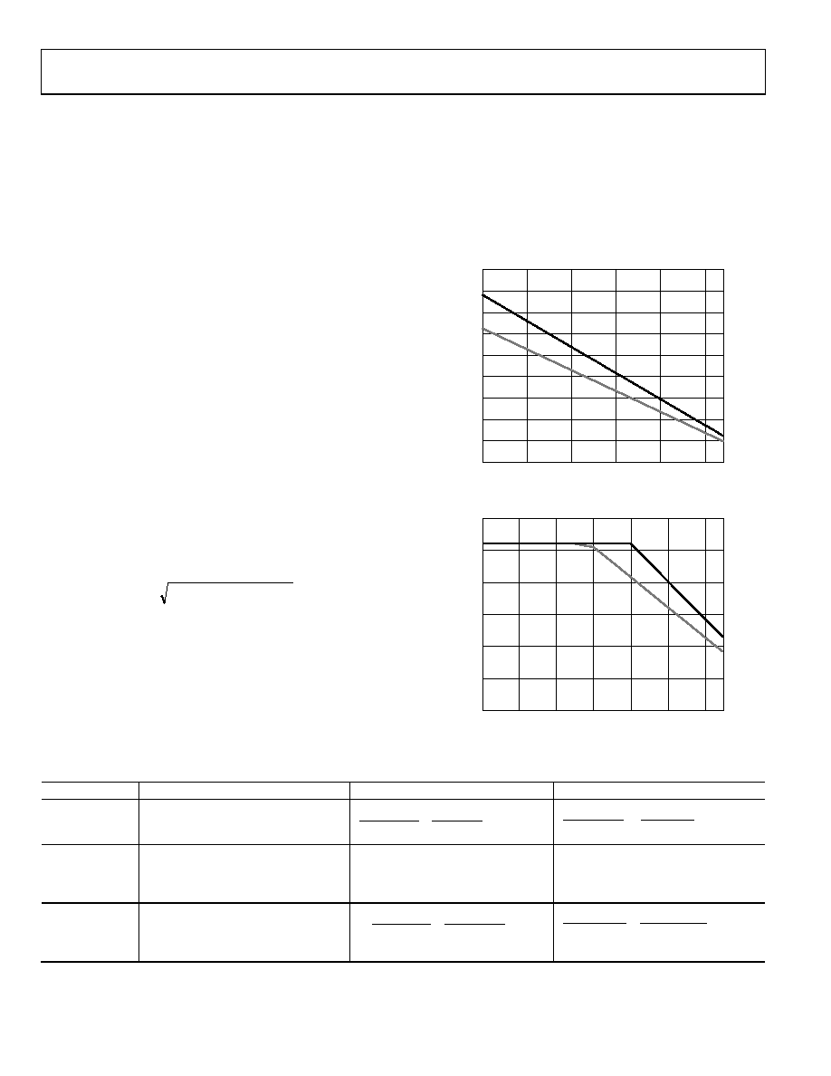
Table 25 provides the bounds of operation at maximum ambient
temperature and maximum supply voltage. This information is
displayed graphically in Figure 52 and Figure 53. These figures
assume that the exposed paddle is connected to a copper plane
of approximately 6 cm2.
4.5
4.0
3.5
3.0
2.5
2.0
1.5
1.0
0.5
0
20
40
60
80
100
PO
W
ER
D
ISSI
PA
T
IO
N
(W
)
AMBIENT TEMPERATURE (°C)
09128-
103
TSSOP
LFCSP
Figure 52. Maximum Power Dissipation vs. Ambient Temperature
60
50
40
30
20
10
0
40
50
60
70
80
90
100
SU
PPL
Y
VO
L
T
A
G
E
(V)
AMBIENT TEMPERATURE (°C)
09128-
102
LFCSP
TSSOP
Figure 53. Maximum Supply Voltage vs. Ambient Temperature
Table 25. Thermal and Supply Considerations (External MOSFET Not Connected)
Parameter
Description
32-Lead LFCSP
28-Lead TSSOP
Maximum
Power
Dissipation
Maximum permitted power
dissipation when operating at an
ambient temperature of 105°C
mW
500
40
105
125
=
=
JA
A
MAX
J
T
θ
mW
625
32
105
125
=
=
JA
A
J MAX
θ
T
Maximum
Ambient
Temperature
Maximum permitted ambient
temperature when operating from a
supply of 52 V while regulating a loop
current of 22.8 mA
=
×
JA
D
MAX
J
P
T
θ
(
)
(
)
C
77
40
0228
.
0
52
125
°
=
×
C
87
)
32
)
0228
.
0
52
((
125
)
(
°
=
×
=
×
JA
D
MAX
J
P
T
θ
Maximum
Supply
Voltage
Maximum permitted supply voltage
when operating at an ambient
temperature of 105°C while regulating
a loop current of 22.8 mA
V
21
40
0228
.
0
105
125
=
×
=
×
JA
LOOP
A
MAX
J
I
T
θ
V
27
32
0228
.
0
105
125
=
×
=
×
JA
LOOP
A
MAX
J
I
T
θ
相关PDF资料 |
PDF描述 |
|---|---|
| AD5422ACPZ-REEL7 | IC DAC 16BIT SRL 40LFCSP |
| AD5441BRMZ-REEL7 | IC DAC 12BIT SERIAL IN 8MSOP |
| AD5445YRU | IC DAC 12BIT PARALL IOUT 20TSSOP |
| AD5446YRM | IC DAC 14BIT MULTIPLYING 10-MSOP |
| AD5447YRU | IC DAC 12BIT DUAL MULT 24-TSSOP |
相关代理商/技术参数 |
参数描述 |
|---|---|
| AD5421CREZ-RL | 功能描述:IC DAC 16BIT SPI/SRL 28TSSOP RoHS:是 类别:集成电路 (IC) >> 数据采集 - 数模转换器 系列:- 标准包装:47 系列:- 设置时间:2µs 位数:14 数据接口:并联 转换器数目:1 电压电源:单电源 功率耗散(最大):55µW 工作温度:-40°C ~ 85°C 安装类型:表面贴装 封装/外壳:28-SSOP(0.209",5.30mm 宽) 供应商设备封装:28-SSOP 包装:管件 输出数目和类型:1 电流,单极;1 电流,双极 采样率(每秒):* |
| AD5421CREZ-RL7 | 功能描述:IC DAC 16BIT SPI/SRL 28TSSOP RoHS:是 类别:集成电路 (IC) >> 数据采集 - 数模转换器 系列:- 标准包装:47 系列:- 设置时间:2µs 位数:14 数据接口:并联 转换器数目:1 电压电源:单电源 功率耗散(最大):55µW 工作温度:-40°C ~ 85°C 安装类型:表面贴装 封装/外壳:28-SSOP(0.209",5.30mm 宽) 供应商设备封装:28-SSOP 包装:管件 输出数目和类型:1 电流,单极;1 电流,双极 采样率(每秒):* |
| AD5422 | 制造商:AD 制造商全称:Analog Devices 功能描述:Single Channel, 12/16-Bit, Serial Input, Current Source & Voltage Output DAC |
| AD5422ACPZ | 制造商:AD 制造商全称:Analog Devices 功能描述:Single Channel, 12/16-Bit, Serial Input, Current Source & Voltage Output DAC |
| AD5422ACPZ-REEL | 功能描述:IC DAC 16BIT SRL 40LFCSP RoHS:是 类别:集成电路 (IC) >> 数据采集 - 数模转换器 系列:- 标准包装:47 系列:- 设置时间:2µs 位数:14 数据接口:并联 转换器数目:1 电压电源:单电源 功率耗散(最大):55µW 工作温度:-40°C ~ 85°C 安装类型:表面贴装 封装/外壳:28-SSOP(0.209",5.30mm 宽) 供应商设备封装:28-SSOP 包装:管件 输出数目和类型:1 电流,单极;1 电流,双极 采样率(每秒):* |
发布紧急采购,3分钟左右您将得到回复。