参数资料
| 型号: | AD5422ACPZ-REEL |
| 厂商: | Analog Devices Inc |
| 文件页数: | 27/44页 |
| 文件大小: | 0K |
| 描述: | IC DAC 16BIT SRL 40LFCSP |
| 设计资源: | 16-Bit Fully Isolated Output Module Using AD5422 and ADuM1401 (CN0065) Simplified 16-Bit Voltage Output and 4 mA-to-20 mA Output Solution Using AD5422 (CN0077) |
| 标准包装: | 2,500 |
| 设置时间: | 25µs |
| 位数: | 16 |
| 数据接口: | MICROWIRE?,串行,SPI? |
| 转换器数目: | 1 |
| 电压电源: | 模拟和数字,双 ± |
| 功率耗散(最大): | 950mW |
| 工作温度: | -40°C ~ 85°C |
| 安装类型: | 表面贴装 |
| 封装/外壳: | 40-VFQFN 裸露焊盘,CSP |
| 供应商设备封装: | 40-LFCSP-VQ(6x6) |
| 包装: | 带卷 (TR) |
| 输出数目和类型: | 1 电流,单极;1 电流,双极;1 电压,单极;1 电压,双极 |
| 采样率(每秒): | 40k |
第1页第2页第3页第4页第5页第6页第7页第8页第9页第10页第11页第12页第13页第14页第15页第16页第17页第18页第19页第20页第21页第22页第23页第24页第25页第26页当前第27页第28页第29页第30页第31页第32页第33页第34页第35页第36页第37页第38页第39页第40页第41页第42页第43页第44页
Data Sheet
AD5412/AD5422
Rev. I | Page 33 of 44
AD5412/AD5422 FEATURES
FAULT ALERT
devices to be connected together to one pull-up resistor for
global fault detection. The FAULT pin is forced active by one
of the following fault scenarios:
The voltage at IOUT attempts to rise above the compliance
range, due to an open-loop circuit or insufficient power
supply voltage. The IOUT current is controlled by a PMOS
transistor and internal amplifier, as shown in Figure 66.
The internal circuitry that develops the fault output avoids
using a comparator with window limits because this would
require an actual output error before the FAULT output
becomes active. Instead, the signal is generated when the
internal amplifier in the output stage has less than ~1 V
of remaining drive capability (when the gate of the output
PMOS transistor nearly reaches ground). Thus, the FAULT
output activates slightly before the compliance limit is
reached. Because the comparison is made within the
feedback loop of the output amplifier, the output accuracy
is maintained by its open-loop gain, and an output error
does not occur before the FAULT output becomes active.
approximately 150°C.
The IOUT fault and over temp bits of the status register are used
in conjunction with the FAULT pin to inform the user which
one of the fault conditions caused the FAULT pin to be asserted
(see Table 19 and Table 20).
VOLTAGE OUTPUT SHORT CIRCUIT PROTECTION
Under normal operation, the voltage output sinks/sources
10 mA. The maximum current that the voltage output delivers
is ~20 mA; this is the short-circuit current.
VOLTAGE OUTPUT OVERRANGE
An overrange facility is provided on the voltage output. When
enabled via the control register, the selected output range is
overranged by, typically, 10%.
VOLTAGE OUTPUT FORCE-SENSE
The +VSENSE and VSENSE pins are provided to facilitate remote
sensing of the load connected to the voltage output. If the load
is connected at the end of a long or high impedance cable,
sensing the voltage at the load allows the output amplifier to
compensate and ensure that the correct voltage is applied across
the load. This function is limited only by the available power
supply headroom.
ASYNCHRONOUS CLEAR (CLEAR)
The CLEAR pin is an active high clear that allows the voltage
output to be cleared to either zero-scale code or midscale code,
user selectable via the CLEAR SELECT pin, or the CLRSEL bit
of the control register, as described in Table 21. (The clear select
feature is a logical OR function of the CLEAR SELECT pin and
the CLRSEL bit.) The current output clears to the bottom of its
programmed range. It is necessary for CLEAR to be high for a
minimum amount of time to complete the operation (see Figure 2).
When the CLEAR signal is returned low, the output remains at
the cleared value. The preclear value can be restored by pulsing
the LATCH signal low without clocking any data. A new value
cannot be programmed until the CLEAR pin is returned low.
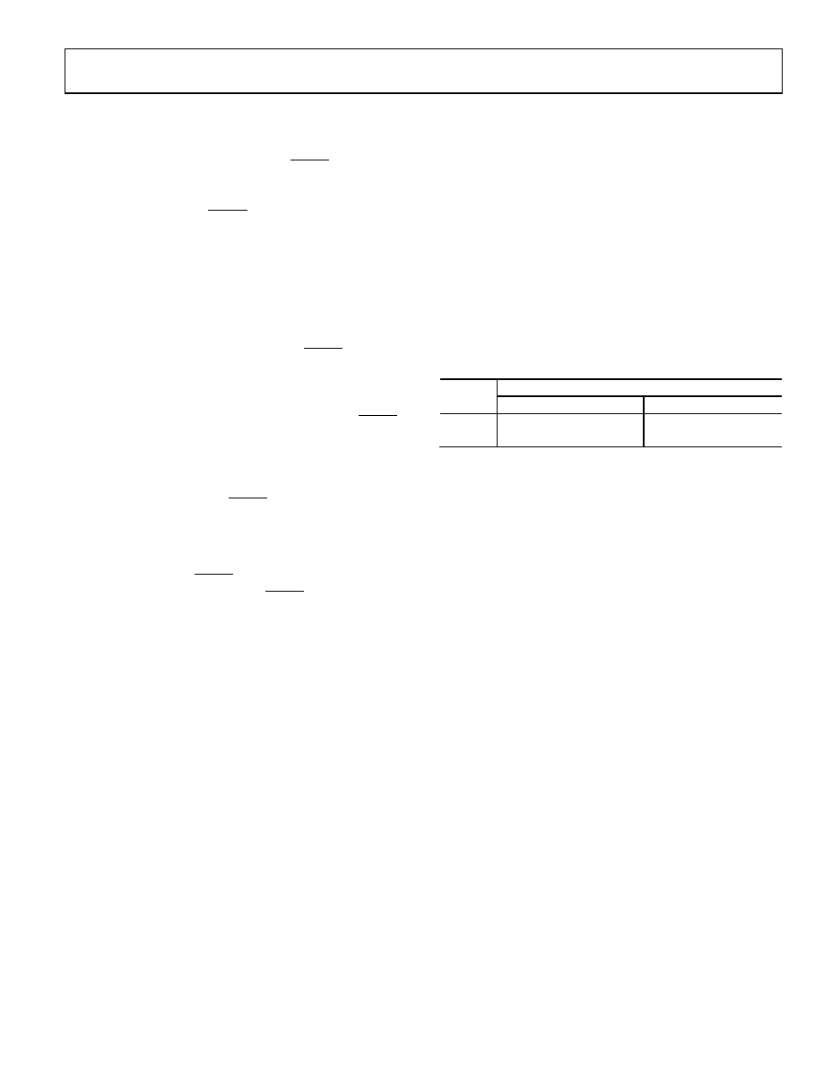
Table 21. CLRSEL Options
CLRSEL
Output Value
Unipolar Output Range
Bipolar Output Range
0
0 V
1
Midscale
Zero scale
In addition to defining the output value for a clear operation,
the CLRSEL bit and CLEAR SELECT pin also define the default
output value. During selection of a new voltage range, the
output value is as defined in Table 21. To avoid glitches on the
output, it is recommended that, before changing voltage ranges,
the user disable the output by setting the OUTEN bit of the
control register to logic low. When OUTEN is set to logic high,
the output goes to the default value as defined by CLRSEL and
CLEAR SELECT.
INTERNAL REFERENCE
reference with initial accuracy of ±5 mV maximum and a
temperature drift coefficient of ±10 ppm/°C maximum. The
reference voltage is buffered and externally available for use
elsewhere within the system. See Figure 16 for a load regulation
graph of the integrated reference.
EXTERNAL CURRENT SETTING RESISTOR
RSET is an internal sense resistor as part of the voltage-to-current
conversion circuitry (see Figure 66). The stability of the output
current over temperature is dependent on the stability of the
value of RSET. As a method of improving the stability of the
output current over temperature, an external precision 15 kΩ
low drift resistor can be connected to the RSET pin of the
(RSET). The external resistor is selected via the control register
(see Table 14).
相关PDF资料 |
PDF描述 |
|---|---|
| VE-J0K-MY | CONVERTER MOD DC/DC 40V 50W |
| AD7305YRZ-REEL | IC DAC 8BIT QUAD R-R 20SOIC |
| VE-JTW-MY | CONVERTER MOD DC/DC 5.5V 50W |
| AD5446YRM-REEL7 | IC DAC 14BIT MULTIPLYING 10-MSOP |
| AD5446YRM-REEL | IC DAC 14BIT MULTIPLYING 10-MSOP |
相关代理商/技术参数 |
参数描述 |
|---|---|
| AD5422ACPZ-REEL7 | 功能描述:IC DAC 16BIT SRL 40LFCSP RoHS:是 类别:集成电路 (IC) >> 数据采集 - 数模转换器 系列:- 标准包装:47 系列:- 设置时间:2µs 位数:14 数据接口:并联 转换器数目:1 电压电源:单电源 功率耗散(最大):55µW 工作温度:-40°C ~ 85°C 安装类型:表面贴装 封装/外壳:28-SSOP(0.209",5.30mm 宽) 供应商设备封装:28-SSOP 包装:管件 输出数目和类型:1 电流,单极;1 电流,双极 采样率(每秒):* |
| AD5422AREZ | 功能描述:IC DAC 16BIT SER 24TSSOP RoHS:是 类别:集成电路 (IC) >> 数据采集 - 数模转换器 系列:- 产品培训模块:Lead (SnPb) Finish for COTS Obsolescence Mitigation Program 标准包装:50 系列:- 设置时间:4µs 位数:12 数据接口:串行 转换器数目:2 电压电源:单电源 功率耗散(最大):- 工作温度:-40°C ~ 85°C 安装类型:表面贴装 封装/外壳:8-TSSOP,8-MSOP(0.118",3.00mm 宽) 供应商设备封装:8-uMAX 包装:管件 输出数目和类型:2 电压,单极 采样率(每秒):* 产品目录页面:1398 (CN2011-ZH PDF) |
| AD5422AREZ-REEL | 功能描述:IC DAC 16BIT SRL 24TSSOP RoHS:是 类别:集成电路 (IC) >> 数据采集 - 数模转换器 系列:- 标准包装:47 系列:- 设置时间:2µs 位数:14 数据接口:并联 转换器数目:1 电压电源:单电源 功率耗散(最大):55µW 工作温度:-40°C ~ 85°C 安装类型:表面贴装 封装/外壳:28-SSOP(0.209",5.30mm 宽) 供应商设备封装:28-SSOP 包装:管件 输出数目和类型:1 电流,单极;1 电流,双极 采样率(每秒):* |
| AD5422BCPZ | 制造商:AD 制造商全称:Analog Devices 功能描述:Single Channel, 16-Bit, Serial Input, Current Source & Voltage Output DAC |
| AD5422BCPZ-REEL | 功能描述:IC DAC 16BIT SRL 40LFCSP RoHS:是 类别:集成电路 (IC) >> 数据采集 - 数模转换器 系列:- 标准包装:47 系列:- 设置时间:2µs 位数:14 数据接口:并联 转换器数目:1 电压电源:单电源 功率耗散(最大):55µW 工作温度:-40°C ~ 85°C 安装类型:表面贴装 封装/外壳:28-SSOP(0.209",5.30mm 宽) 供应商设备封装:28-SSOP 包装:管件 输出数目和类型:1 电流,单极;1 电流,双极 采样率(每秒):* |
发布紧急采购,3分钟左右您将得到回复。