- 您现在的位置:买卖IC网 > PDF目录8724 > AD5444YRMZ-REEL (Analog Devices Inc)IC DAC 12BIT MULTIPLYING 10-MSOP PDF资料下载
参数资料
| 型号: | AD5444YRMZ-REEL |
| 厂商: | Analog Devices Inc |
| 文件页数: | 28/29页 |
| 文件大小: | 0K |
| 描述: | IC DAC 12BIT MULTIPLYING 10-MSOP |
| 产品培训模块: | Data Converter Fundamentals DAC Architectures |
| 标准包装: | 3,000 |
| 设置时间: | 16ns |
| 位数: | 12 |
| 数据接口: | 串行 |
| 转换器数目: | 1 |
| 电压电源: | 单电源 |
| 功率耗散(最大): | 50.5µW |
| 工作温度: | -40°C ~ 125°C |
| 安装类型: | 表面贴装 |
| 封装/外壳: | 10-TFSOP,10-MSOP(0.118",3.00mm 宽) |
| 供应商设备封装: | 10-MSOP |
| 包装: | 带卷 (TR) |
| 输出数目和类型: | 2 电流,单极;2 电流,双极 |
| 采样率(每秒): | 2.7M |
第1页第2页第3页第4页第5页第6页第7页第8页第9页第10页第11页第12页第13页第14页第15页第16页第17页第18页第19页第20页第21页第22页第23页第24页第25页第26页第27页当前第28页第29页
Data Sheet
AD5444/AD5446
Rev. E | Page 7 of 28
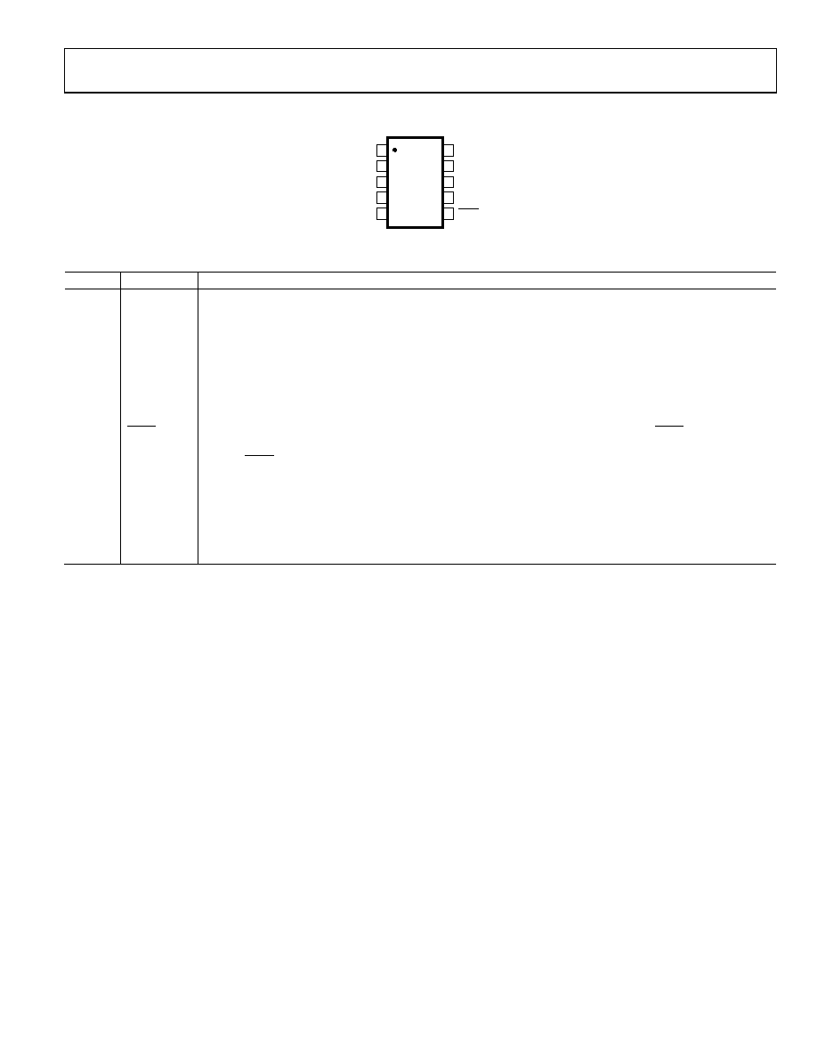
PIN CONFIGURATION AND FUNCTION DESCRIPTIONS
04588-
005
10
9
8
7
6
1
2
3
4
5
IOUT1
IOUT2
GND
SCLK
SDIN
RFB
VREF
VDD
SDO
AD5444/
AD5446
TOP VIEW
(Not to Scale)
SYNC
Figure 5. Pin Configuration
Table 4. Pin Function Descriptions
Pin No.
Mnemonic
Description
1
IOUT1
DAC Current Output.
2
IOUT2
DAC Analog Ground. This pin should normally be tied to the analog ground of the system.
3
GND
Ground Pin.
4
SCLK
Serial Clock Input. By default, data is clocked into the input shift register on the falling edge of the serial clock
input. Alternatively, by means of the serial control bits, the device can be configured such that data is clocked
into the shift register on the rising edge of SCLK.
5
SDIN
Serial Data Input. Data is clocked into the 16-bit input register on the active edge of the serial clock input.
By default on power-up, data is clocked into the shift register on the falling edge of SCLK. The control bits allow
the user to change the active edge to the rising edge.
6
SYNC
Active Low Control Input. This is the frame synchronization signal for the input data. When SYNC is taken low,
data is loaded to the shift register on the active edge of the following clocks. The output updates on the rising
edge of SYNC.
7
SDO
Serial Data Output. This pin allows a number of parts to be daisy-chained. By default, data is clocked into the shift
register on the falling edge and out via SDO on the rising edge of SCLK. Data is always clocked out on the
alternate edge to data loaded to the shift register.
8
VDD
Positive Power Supply Input. This part can be operated from a supply of 2.5 V to 5.5 V.
9
VREF
DAC Reference Voltage Input.
10
RFB
DAC Feedback Resistor. Establishes voltage output for the DAC by connecting to an external amplifier output.
相关PDF资料 |
PDF描述 |
|---|---|
| V24A5H400BG2 | CONVERTER MOD DC/DC 5V 400W |
| AD5445YRUZ-REEL7 | IC DAC 12BIT PARALL IOUT 20TSSOP |
| V24A5H400BF2 | CONVERTER MOD DC/DC 5V 400W |
| V24A5H400BL3 | CONVERTER MOD DC/DC 5V 400W |
| VE-22X-MW-F3 | CONVERTER MOD DC/DC 5.2V 100W |
相关代理商/技术参数 |
参数描述 |
|---|---|
| AD5444YRMZ-REEL7 | 功能描述:IC DAC 12BIT MULTIPLYING 10-MSOP RoHS:是 类别:集成电路 (IC) >> 数据采集 - 数模转换器 系列:- 产品培训模块:LTC263x 12-, 10-, and 8-Bit VOUT DAC Family 特色产品:LTC2636 - Octal 12-/10-/8-Bit SPI VOUT DACs with 10ppm/°C Reference 标准包装:91 系列:- 设置时间:4µs 位数:10 数据接口:MICROWIRE?,串行,SPI? 转换器数目:8 电压电源:单电源 功率耗散(最大):2.7mW 工作温度:-40°C ~ 85°C 安装类型:表面贴装 封装/外壳:14-WFDFN 裸露焊盘 供应商设备封装:14-DFN-EP(4x3) 包装:管件 输出数目和类型:8 电压,单极 采样率(每秒):* |
| AD5445 | 制造商:AD 制造商全称:Analog Devices 功能描述:Dual 8-,10-,12-Bit High Bandwidth Multiplying DACs with Serial Interface |
| AD5445YCP | 制造商:Analog Devices 功能描述:DAC 1-CH R-2R 12-bit 20-Pin LFCSP EP 制造商:Rochester Electronics LLC 功能描述:12-BIT LOUT DAC PARELLED INT/FACE I.C. - Bulk 制造商:Analog Devices 功能描述:12BIT DAC PARALLEL I/F SMD 5445 |
| AD5445YCP-REEL | 制造商:Analog Devices 功能描述:DAC 1-CH R-2R 12-bit 20-Pin LFCSP EP T/R |
| AD5445YCP-REEL7 | 制造商:Analog Devices 功能描述:DAC 1-CH R-2R 12-bit 20-Pin LFCSP EP T/R 制造商:Rochester Electronics LLC 功能描述:12-BIT LOUT DAC PARELLED INT/FACE I.C. - Tape and Reel |
发布紧急采购,3分钟左右您将得到回复。