参数资料
| 型号: | AD5446YRMZ |
| 厂商: | Analog Devices Inc |
| 文件页数: | 11/29页 |
| 文件大小: | 0K |
| 描述: | IC DAC 14BIT MULTIPLYING 10-MSOP |
| 产品培训模块: | Data Converter Fundamentals DAC Architectures |
| 设计资源: | Versatile High Precision Programmable Current Sources Using DACs, Op Amps, and MOSFET Transistors (CN0151) |
| 标准包装: | 50 |
| 位数: | 14 |
| 数据接口: | DSP,MICROWIRE?,QSPI?,串行,SPI? |
| 转换器数目: | 1 |
| 电压电源: | 单电源 |
| 功率耗散(最大): | 50.5µW |
| 工作温度: | -40°C ~ 125°C |
| 安装类型: | 表面贴装 |
| 封装/外壳: | 10-TFSOP,10-MSOP(0.118",3.00mm 宽) |
| 供应商设备封装: | 10-MSOP |
| 包装: | 管件 |
| 输出数目和类型: | 2 电流,单极;2 电流,双极 |
| 采样率(每秒): | 2.7M |
| 产品目录页面: | 782 (CN2011-ZH PDF) |
| 配用: | EVAL-AD5446EBZ-ND - BOARD EVALUATION FOR AD5446 |
第1页第2页第3页第4页第5页第6页第7页第8页第9页第10页当前第11页第12页第13页第14页第15页第16页第17页第18页第19页第20页第21页第22页第23页第24页第25页第26页第27页第28页第29页
AD5444/AD5446
Data Sheet
Rev. E | Page 18 of 28
04588-
035
NOTES:
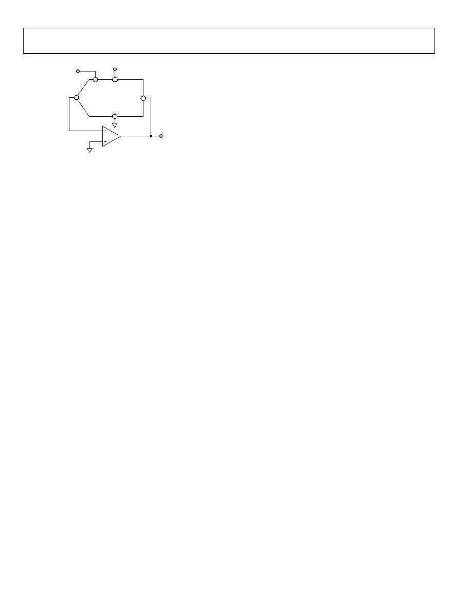
1. ADDITIONAL PINS OMITTED FOR CLARITY.
IOUT1
GND
VOUT
VIN
RFB
VDD
VREF
VDD
Figure 43. Current-Steering DAC Used as a Divider
or Programmable Gain Element
As D is reduced, the output voltage increases. For small values
of the digital fraction (D), it is important to ensure that the
amplifier does not saturate and the required accuracy is met.
For example, an 8-bit DAC driven with the binary code 0x10
(0001 0000), that is, 16 decimal, in the circuit of Figure 43,
should cause the output voltage to be 16 × VIN. However, if the
DAC has a linearity specification of ±0.5 LSB, then D can, in
fact, have a weight in the range of 15.5/256 to 16.5/256, so the
possible output voltage is in the range 15.5 VIN to 16.5 VIN. This
is an error of 3%, even though the DAC itself has a maximum
error of 0.2%.
DAC leakage current is also a potential error source in divider
circuits. The leakage current must be counterbalanced by an
opposite current supplied from the op amp through the DAC.
Because only a fraction (D) of the current into the VREF terminal
is routed to the IOUT1 terminal, the output voltage has to change,
as follows:
Output Error Voltage due to DAC Leakage = (Leakage × R)/D
where R is the DAC resistance at the VREF terminal.
For a DAC leakage current of 10 nA, R equal to 10 k, and a gain
(1/D) of 16, the error voltage is 1.6 mV.
AMPLIFIER SELECTION
The primary requirement for the current-steering mode is
an amplifier with low input bias currents and low input offset
voltage. The input offset voltage of an op amp is multiplied by
the variable gain (due to the code-dependent output resistance
of the DAC) of the circuit. A change in this noise gain between
two adjacent digital fractions produces a step change in the
output voltage due to the amplifier’s input offset voltage. This
output voltage change is superimposed upon the desired change
in output between the two codes and gives rise to a differential
linearity error, which, if large enough, can cause the DAC to be
nonmonotonic.
The input bias current of an op amp also generates an offset
at the voltage output as a result of the bias current flowing
in the feedback resistor, RFB. Most op amps have input bias
currents low enough to prevent any significant errors in
12-bit applications.
Common-mode rejection of the op amp is important in voltage
switching circuits because it produces a code-dependent error
at the voltage output of the circuit. Most op amps have adequate
common-mode rejection for use at 8-bit, 10-bit, and 12-bit
resolutions.
Provided that the DAC switches are driven from true wideband
low impedance sources (VIN and AGND), they settle quickly.
Consequently, the slew rate and settling time of a voltage switching
DAC circuit is determined largely by the output op amp. To
obtain minimum settling time in this configuration, it is impor-
tant to minimize capacitance at the VREF node (voltage output
node in this application) of the DAC. This is done by using low
input, capacitance buffer amplifiers and careful board design.
Most single-supply circuits include ground as part of the analog
signal range, which, in turn, requires an amplifier that can handle
rail-to-rail signals. A large range of single-supply amplifiers is
available from Analog Devices, Inc. (see Table 8 and Table 9 for
suitable suggestions).
REFERENCE SELECTION
When selecting a reference for use with the AD5444/AD5446
current output DAC, pay attention to the output voltage tem-
perature coefficient specification. This parameter affects not
only the full-scale error but can also affect the linearity (INL
and DNL) performance. The reference temperature coefficient
should be consistent with the system accuracy specifications.
For example, an 8-bit system required to hold its overall speci-
fication to within 1 LSB over the temperature range 0°C to 50°C
dictates that the maximum system drift with temperature
should be less than 78 ppm/°C.
A 12-bit system with the same temperature range to overall
specification within 2 LSBs requires a maximum drift of
10 ppm/°C. By choosing a precision reference with low output
temperature coefficient, this error source can be minimized.
Table 7 suggests some of the dc references available from
Analog Devices that are suitable for use with this range of
current output DACs.
相关PDF资料 |
PDF描述 |
|---|---|
| ICS841654AGILFT | IC CLOCK GENERATOR 28-TSSOP |
| VI-B0T-MY-F1 | CONVERTER MOD DC/DC 6.5V 50W |
| VE-J0P-MZ-F3 | CONVERTER MOD DC/DC 13.8V 25W |
| VI-JT1-MZ-F3 | CONVERTER MOD DC/DC 12V 25W |
| AD5060ARJZ-2500RL7 | IC DAC 16BIT SPI/SRL SOT23-8 |
相关代理商/技术参数 |
参数描述 |
|---|---|
| AD5446YRMZ-RL7 | 功能描述:IC DAC 14BIT SRL 10MSOP RoHS:是 类别:集成电路 (IC) >> 数据采集 - 数模转换器 系列:- 产品培训模块:LTC263x 12-, 10-, and 8-Bit VOUT DAC Family 特色产品:LTC2636 - Octal 12-/10-/8-Bit SPI VOUT DACs with 10ppm/°C Reference 标准包装:91 系列:- 设置时间:4µs 位数:10 数据接口:MICROWIRE?,串行,SPI? 转换器数目:8 电压电源:单电源 功率耗散(最大):2.7mW 工作温度:-40°C ~ 85°C 安装类型:表面贴装 封装/外壳:14-WFDFN 裸露焊盘 供应商设备封装:14-DFN-EP(4x3) 包装:管件 输出数目和类型:8 电压,单极 采样率(每秒):* |
| AD5447 | 制造商:AD 制造商全称:Analog Devices 功能描述:Dual 8-,10-,12-Bit High Bandwidth Multiplying DACs with Serial Interface |
| AD5447YRU | 功能描述:IC DAC 12BIT DUAL MULT 24-TSSOP RoHS:否 类别:集成电路 (IC) >> 数据采集 - 数模转换器 系列:- 标准包装:47 系列:- 设置时间:2µs 位数:14 数据接口:并联 转换器数目:1 电压电源:单电源 功率耗散(最大):55µW 工作温度:-40°C ~ 85°C 安装类型:表面贴装 封装/外壳:28-SSOP(0.209",5.30mm 宽) 供应商设备封装:28-SSOP 包装:管件 输出数目和类型:1 电流,单极;1 电流,双极 采样率(每秒):* |
| AD5447YRU-REEL | 功能描述:IC DAC 12BIT DUAL MULT 24-TSSOP RoHS:否 类别:集成电路 (IC) >> 数据采集 - 数模转换器 系列:- 产品培训模块:LTC263x 12-, 10-, and 8-Bit VOUT DAC Family 特色产品:LTC2636 - Octal 12-/10-/8-Bit SPI VOUT DACs with 10ppm/°C Reference 标准包装:91 系列:- 设置时间:4µs 位数:10 数据接口:MICROWIRE?,串行,SPI? 转换器数目:8 电压电源:单电源 功率耗散(最大):2.7mW 工作温度:-40°C ~ 85°C 安装类型:表面贴装 封装/外壳:14-WFDFN 裸露焊盘 供应商设备封装:14-DFN-EP(4x3) 包装:管件 输出数目和类型:8 电压,单极 采样率(每秒):* |
| AD5447YRU-REEL7 | 制造商:Analog Devices 功能描述:DAC 2-CH R-2R 12-bit 24-Pin TSSOP T/R 制造商:Analog Devices 功能描述:DAC 2CH R-2R 12-BIT 24TSSOP - Tape and Reel |
发布紧急采购,3分钟左右您将得到回复。