参数资料
| 型号: | AD5446YRMZ |
| 厂商: | Analog Devices Inc |
| 文件页数: | 15/29页 |
| 文件大小: | 0K |
| 描述: | IC DAC 14BIT MULTIPLYING 10-MSOP |
| 产品培训模块: | Data Converter Fundamentals DAC Architectures |
| 设计资源: | Versatile High Precision Programmable Current Sources Using DACs, Op Amps, and MOSFET Transistors (CN0151) |
| 标准包装: | 50 |
| 位数: | 14 |
| 数据接口: | DSP,MICROWIRE?,QSPI?,串行,SPI? |
| 转换器数目: | 1 |
| 电压电源: | 单电源 |
| 功率耗散(最大): | 50.5µW |
| 工作温度: | -40°C ~ 125°C |
| 安装类型: | 表面贴装 |
| 封装/外壳: | 10-TFSOP,10-MSOP(0.118",3.00mm 宽) |
| 供应商设备封装: | 10-MSOP |
| 包装: | 管件 |
| 输出数目和类型: | 2 电流,单极;2 电流,双极 |
| 采样率(每秒): | 2.7M |
| 产品目录页面: | 782 (CN2011-ZH PDF) |
| 配用: | EVAL-AD5446EBZ-ND - BOARD EVALUATION FOR AD5446 |
第1页第2页第3页第4页第5页第6页第7页第8页第9页第10页第11页第12页第13页第14页当前第15页第16页第17页第18页第19页第20页第21页第22页第23页第24页第25页第26页第27页第28页第29页
Data Sheet
AD5444/AD5446
Rev. E | Page 21 of 28
MICROPROCESSOR INTERFACING
Microprocessor interfacing to the AD5444/AD5446 DAC is
through a serial bus that uses standard protocol compatible
with microcontrollers and DSP processors. The communica-
tions channel is a 3-wire interface consisting of a clock signal, a
data signal, and a synchronization signal. The AD5444/AD5446
requires a 16-bit word, with the default being data valid on the
falling edge of SCLK, but this can be changed using the control
bits in the data-word.
ADSP-21xx to AD5444/AD5446 Interface
The ADSP-21xx family of DSPs is easily interfaced to the
AD5444/AD5446 DAC without the need for extra glue logic.
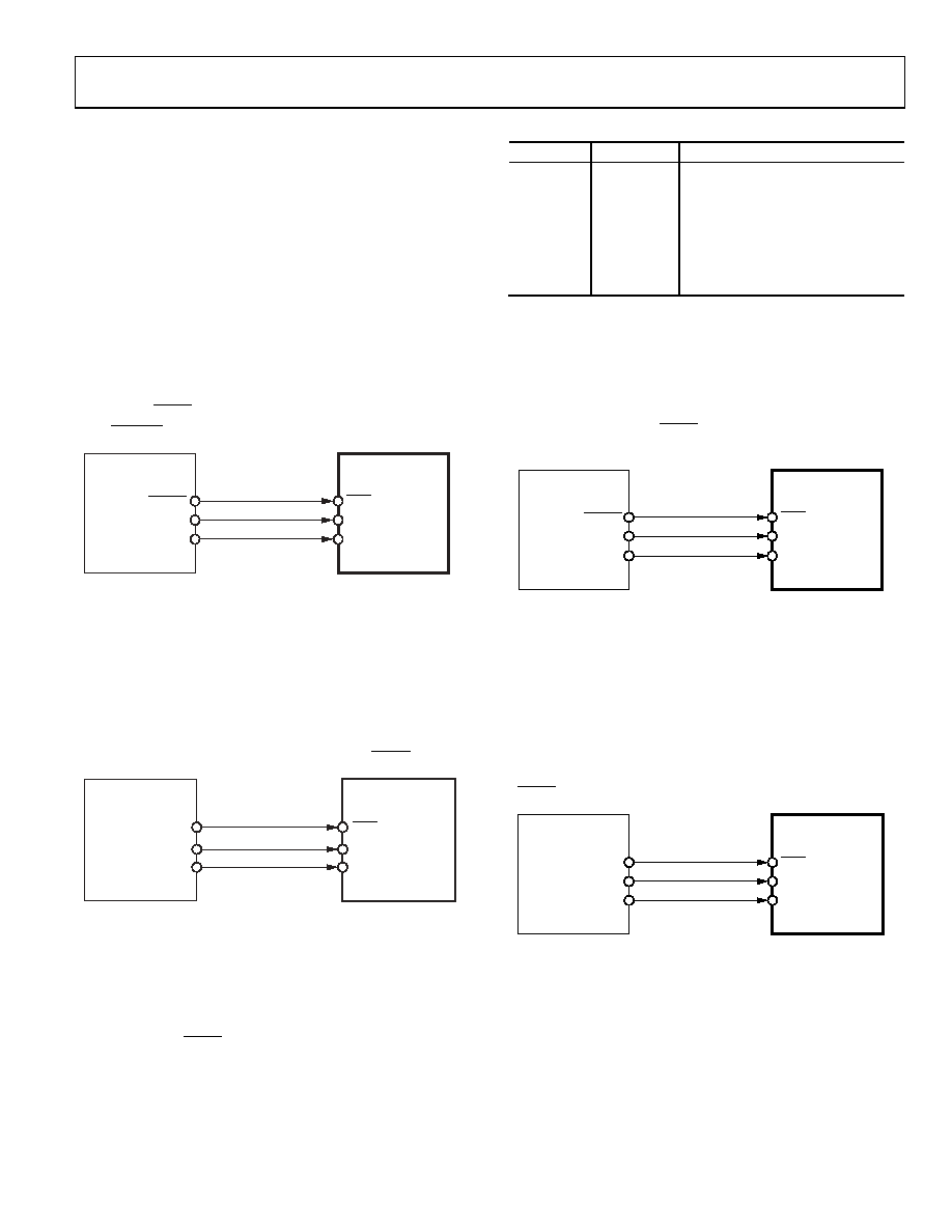
Figure 46 is an example of an SPI interface between the DAC
and the ADSP-2191M. SCK of the DSP drives the serial clock
line, SCLK. SYNC is driven from one of the port lines, in this
case SPIxSEL.
SCLK
SCK
SYNC
SPIxSEL
SDIN
MOSI
ADSP-2191M*
*ADDITIONAL PINS OMITTED FOR CLARITY.
AD5444/
AD5446*
0
4588-
074
Figure 46. ADSP-2191M SPI to AD5444/AD5446 Interface
A serial interface between the DAC and DSP SPORT is shown
in Figure 47. In this interface example, SPORT0 is used to trans-
fer data to the DAC shift register. Transmission is initiated by
writing a word to the Tx register after the SPORT has been
enabled. In a write sequence, data is clocked out on each rising
edge of the DSP serial clock and clocked into the DAC input
shift register on the falling edge of its SCLK. The update of the
DAC output takes place on the rising edge of the SYNC signal.
SCLK
SYNC
TFS
SDIN
DT
ADSP-2101/
ADSP-2191M*
*ADDITIONAL PINS OMITTED FOR CLARITY.
0
458
8-
0
82
AD5444/AD5446*
Figure 47. ADSP-2101/ADSP-2191M to
AD5444/AD5446 Interface
Communication between two devices at a given clock speed
is possible when the following specifications are compatible:
frame sync delay and frame sync setup-and-hold, data delay
and data setup-and-hold, and SCLK width. The DAC inter-
face expects a t4 (SYNC falling edge to SCLK falling edge setup
time) of 13 ns minimum. See the ADSP-21xx User Manual for
information on clock and frame sync frequencies for the
SPORT register.
Table 11 shows the setup for the SPORT control register.
Table 11. SPORT Control Register Setup
Name
Setting
Description
TFSW
1
Alternate framing
INVTFS
1
Active low frame signal
DTYPE
00
Right-justify data
ISCLK
1
Internal serial clock
TFSR
1
Frame every word
ITFS
1
Internal framing signal
SLEN
1111
16-bit data-word
ADSP-BF5xx to AD5444/AD5446 Interface
The ADSP-BF5xx family of processors has an SPI-compatible
port that enables the processor to communicate with SPI-
compatible devices. A serial interface between the ADSP-BF5xx
and the AD5444/AD5446 DAC is shown in Figure 48. In this
configuration, data is transferred through the MOSI (master
output/slave input) pin. SYNC is driven by the SPI chip select
pin, which is a reconfigured programmable flag pin.
SCLK
SCK
SYNC
SPIxSEL
SDIN
MOSI
ADSP-BF5xx*
*ADDITIONAL PINS OMITTED FOR CLARITY
AD5444/AD5446*
0
4588-
039
Figure 48. ADSP-BF5xx to AD5444/AD5446 Interface
The ADSP-BF5xx processor incorporates channel synchronous
serial ports (SPORT). A serial interface between the DAC and
the DSP SPORT is shown in Figure 49. When the SPORT is
enabled, initiate transmission by writing a word to the Tx register.
The data is clocked out on each rising edge of the DSPs serial
clock and clocked into the DAC input shift register on the
falling edge of its SCLK. The DAC output is updated by using
the transmit frame synchronization (TFS) line to provide a
SYNC signal.
SCLK
SYNC
TFS
SDIN
DT
ADSP-BF5xx*
*ADDITIONAL PINS OMITTED FOR CLARITY
04588-
040
AD5444/AD5446*
Figure 49. ADSP-BF5xx to AD5444/AD5446 Interface
相关PDF资料 |
PDF描述 |
|---|---|
| ICS841654AGILFT | IC CLOCK GENERATOR 28-TSSOP |
| VI-B0T-MY-F1 | CONVERTER MOD DC/DC 6.5V 50W |
| VE-J0P-MZ-F3 | CONVERTER MOD DC/DC 13.8V 25W |
| VI-JT1-MZ-F3 | CONVERTER MOD DC/DC 12V 25W |
| AD5060ARJZ-2500RL7 | IC DAC 16BIT SPI/SRL SOT23-8 |
相关代理商/技术参数 |
参数描述 |
|---|---|
| AD5446YRMZ-RL7 | 功能描述:IC DAC 14BIT SRL 10MSOP RoHS:是 类别:集成电路 (IC) >> 数据采集 - 数模转换器 系列:- 产品培训模块:LTC263x 12-, 10-, and 8-Bit VOUT DAC Family 特色产品:LTC2636 - Octal 12-/10-/8-Bit SPI VOUT DACs with 10ppm/°C Reference 标准包装:91 系列:- 设置时间:4µs 位数:10 数据接口:MICROWIRE?,串行,SPI? 转换器数目:8 电压电源:单电源 功率耗散(最大):2.7mW 工作温度:-40°C ~ 85°C 安装类型:表面贴装 封装/外壳:14-WFDFN 裸露焊盘 供应商设备封装:14-DFN-EP(4x3) 包装:管件 输出数目和类型:8 电压,单极 采样率(每秒):* |
| AD5447 | 制造商:AD 制造商全称:Analog Devices 功能描述:Dual 8-,10-,12-Bit High Bandwidth Multiplying DACs with Serial Interface |
| AD5447YRU | 功能描述:IC DAC 12BIT DUAL MULT 24-TSSOP RoHS:否 类别:集成电路 (IC) >> 数据采集 - 数模转换器 系列:- 标准包装:47 系列:- 设置时间:2µs 位数:14 数据接口:并联 转换器数目:1 电压电源:单电源 功率耗散(最大):55µW 工作温度:-40°C ~ 85°C 安装类型:表面贴装 封装/外壳:28-SSOP(0.209",5.30mm 宽) 供应商设备封装:28-SSOP 包装:管件 输出数目和类型:1 电流,单极;1 电流,双极 采样率(每秒):* |
| AD5447YRU-REEL | 功能描述:IC DAC 12BIT DUAL MULT 24-TSSOP RoHS:否 类别:集成电路 (IC) >> 数据采集 - 数模转换器 系列:- 产品培训模块:LTC263x 12-, 10-, and 8-Bit VOUT DAC Family 特色产品:LTC2636 - Octal 12-/10-/8-Bit SPI VOUT DACs with 10ppm/°C Reference 标准包装:91 系列:- 设置时间:4µs 位数:10 数据接口:MICROWIRE?,串行,SPI? 转换器数目:8 电压电源:单电源 功率耗散(最大):2.7mW 工作温度:-40°C ~ 85°C 安装类型:表面贴装 封装/外壳:14-WFDFN 裸露焊盘 供应商设备封装:14-DFN-EP(4x3) 包装:管件 输出数目和类型:8 电压,单极 采样率(每秒):* |
| AD5447YRU-REEL7 | 制造商:Analog Devices 功能描述:DAC 2-CH R-2R 12-bit 24-Pin TSSOP T/R 制造商:Analog Devices 功能描述:DAC 2CH R-2R 12-BIT 24TSSOP - Tape and Reel |
发布紧急采购,3分钟左右您将得到回复。