参数资料
| 型号: | AD5501BRUZ |
| 厂商: | Analog Devices Inc |
| 文件页数: | 20/20页 |
| 文件大小: | 0K |
| 描述: | IC DAC 12BIT SPI 16-TSSOP |
| 产品培训模块: | DAC Architectures |
| 标准包装: | 96 |
| 设置时间: | 45µs |
| 位数: | 12 |
| 数据接口: | SPI?、QSPI?、MICROWIRE? 和 DSP |
| 转换器数目: | 1 |
| 电压电源: | 单 |
| 工作温度: | -40°C ~ 105°C |
| 安装类型: | * |
| 封装/外壳: | 16-TSSOP(0.173",4.40mm 宽) |
| 供应商设备封装: | * |
| 包装: | 管件 |
| 输出数目和类型: | 1 电压,单极 |
| 采样率(每秒): | * |
Data Sheet
AD5501
Rev. C | Page 9 of 20
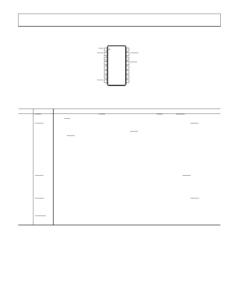
PIN CONFIGURATION AND FUNCTION DESCRIPTIONS
NC = NO CONNECT
1
2
3
4
5
6
7
8
SYNC
SCLK
SDI
AGND
DGND
SDO
CLR
LDAC
16
15
14
13
12
11
10
9
ALARM
VDD
R_SEL
NC
VFB
VOUT
VLOGIC
TOP VIEW
(Not to Scale)
AD5501
07992-
005
Figure 5. Pin Configuration
Table 7. Pin Function Descriptions
Pin No.
Mnemonic
Description
1
CLR
Asynchronous Clear Input. The CLR input is falling edge sensitive. When CLR is low, all LDAC pulses are ignored.
When CLR is activated, the input register and the DAC register are set to 0x000 and the output to zero scale.
2
SYNC
Falling Edge Synchronization Signal. This is the frame synchronization signal for the input data. When SYNC goes low, it
enables the input shift register and data is transferred in on the rising edges of the following clocks. The selected
DAC register is updated on the 16th falling SCLK, unless SYNC is taken high before this edge, in which case, the rising
edge of SYNC acts as an interrupt, and the write sequence is ignored by the DAC.
3
SCLK
Serial Data Input. This part has a 16-bit shift register. Data is clocked into the register on the rising edge of the serial
clock input.
4
SDI
Serial Data Input. This part has a 16-bit shift register. Data is clocked into the register on the falling edge of the serial clock
input.
5
SDO
Serial Data Output. CMOS output. This pin serves as the readback function for all DAC and control registers. Data is
clocked out on the rising edge of SCLK and is valid on the falling edge of SCLK.
6
DGND
Digital Ground Pin.
7
AGND
Analog Ground Pin.
8
LDAC
Load DAC Input. Pulsing this pin low updates the DAC with the value in the input register. If the LDAC pin is tied low, the
DAC output is updated automatically when data is written to the input register.
9, 10
NC
Not Connected. These pins remain unconnected.
11
V
FB
Voltage Feedback Pin. Feedback node for the output amplifier.
12
V
OUT
Buffered Analog Output Voltage from the DAC.
13
R_SEL
Range Select Pin. Tying this pin to DGND selects a DAC output range of 0 V to 60 V, alternatively tying R_SEL to VLOGIC
selects a DAC output range of 0 V to 30 V.
14
V
DD
Positive Analog Power Supply. 10 V to 62 V for the specified performance. Decouple this pin with 0.1F ceramic
capacitors and 10 F capacitors.
15
ALARM
Active Low CMOS Output Pin. Flags an alarm if the temperature on the die exceeds 110°C.
16
V
LOGIC
Logic Power Supply; 2.3 V to 5.5 V. Decouple this with 0.1 F ceramic capacitors and 10 F capacitors.
相关PDF资料 |
PDF描述 |
|---|---|
| AD5520JSTZ | IC PPMU SNGL-CH 64-LQFP |
| AD5522JSVUZ | IC PMU QUAD 16BIT DAC 80-TQFP |
| AD5532ABC-5 | IC DAC 14BIT 32CH 74-CSPBGA |
| AD5532HSABC | IC DAC 14BIT 32CH 74-CSPBGA |
| AD5535ABCZ | IC DAC 14BIT 32CHAN 124CSPBGA |
相关代理商/技术参数 |
参数描述 |
|---|---|
| AD5501BRUZ | 制造商:Analog Devices 功能描述:IC DAC 12BIT TSSOP-16 |
| AD5501BRUZ-REEL | 功能描述:12 Bit Digital to Analog Converter 1 16-TSSOP 制造商:analog devices inc. 系列:- 包装:带卷(TR) 零件状态:上次购买时间 位数:12 数模转换器数:1 建立时间:55μs 输出类型:Voltage - Buffered 差分输出:无 数据接口:SPI,DSP 参考类型:内部 电压 - 电源,模拟:10 V ~ 62 V 电压 - 电源,数字:2.3 V ~ 5.5 V INL/DNL(LSB):±2(最大),±1(最大) 架构:电阻串 DAC 工作温度:-40°C ~ 105°C 封装/外壳:16-TSSOP(0.173",4.40mm 宽) 供应商器件封装:16-TSSOP 标准包装:1 |
| AD5504BRUZ | 功能描述:IC DAC 12BIT SPI 16-TSSOP RoHS:是 类别:集成电路 (IC) >> 数据采集 - 数模转换器 系列:- 标准包装:1 系列:- 设置时间:4.5µs 位数:12 数据接口:串行,SPI? 转换器数目:1 电压电源:单电源 功率耗散(最大):- 工作温度:-40°C ~ 125°C 安装类型:表面贴装 封装/外壳:8-SOIC(0.154",3.90mm 宽) 供应商设备封装:8-SOICN 包装:剪切带 (CT) 输出数目和类型:1 电压,单极;1 电压,双极 采样率(每秒):* 其它名称:MCP4921T-E/SNCTMCP4921T-E/SNRCTMCP4921T-E/SNRCT-ND |
| AD5504BRUZ-REEL | 制造商:AD 制造商全称:Analog Devices 功能描述:High Voltage, Quad-Channel 12-Bit Voltage Output DAC |
| AD5512A | 制造商:AD 制造商全称:Analog Devices 功能描述:2.7 V to 5.5 V, Serial-Input, Voltage-Output, 16-/12-Bit nanoDACs in LFCSP |
发布紧急采购,3分钟左右您将得到回复。