参数资料
| 型号: | AD5530BRUZ |
| 厂商: | Analog Devices Inc |
| 文件页数: | 19/20页 |
| 文件大小: | 0K |
| 描述: | IC DAC 12BIT SRL IN/VOUT 16TSSOP |
| 产品培训模块: | Data Converter Fundamentals DAC Architectures |
| 标准包装: | 96 |
| 设置时间: | 20µs |
| 位数: | 12 |
| 数据接口: | 串行 |
| 转换器数目: | 1 |
| 电压电源: | 模拟和数字 |
| 功率耗散(最大): | 60mW |
| 工作温度: | -40°C ~ 85°C |
| 安装类型: | 表面贴装 |
| 封装/外壳: | 16-TSSOP(0.173",4.40mm 宽) |
| 供应商设备封装: | 16-TSSOP |
| 包装: | 管件 |
| 输出数目和类型: | 1 电压,双极 |
| 采样率(每秒): | 50k |
| 产品目录页面: | 782 (CN2011-ZH PDF) |
AD5530/AD5531
Rev. B | Page 8 of 20
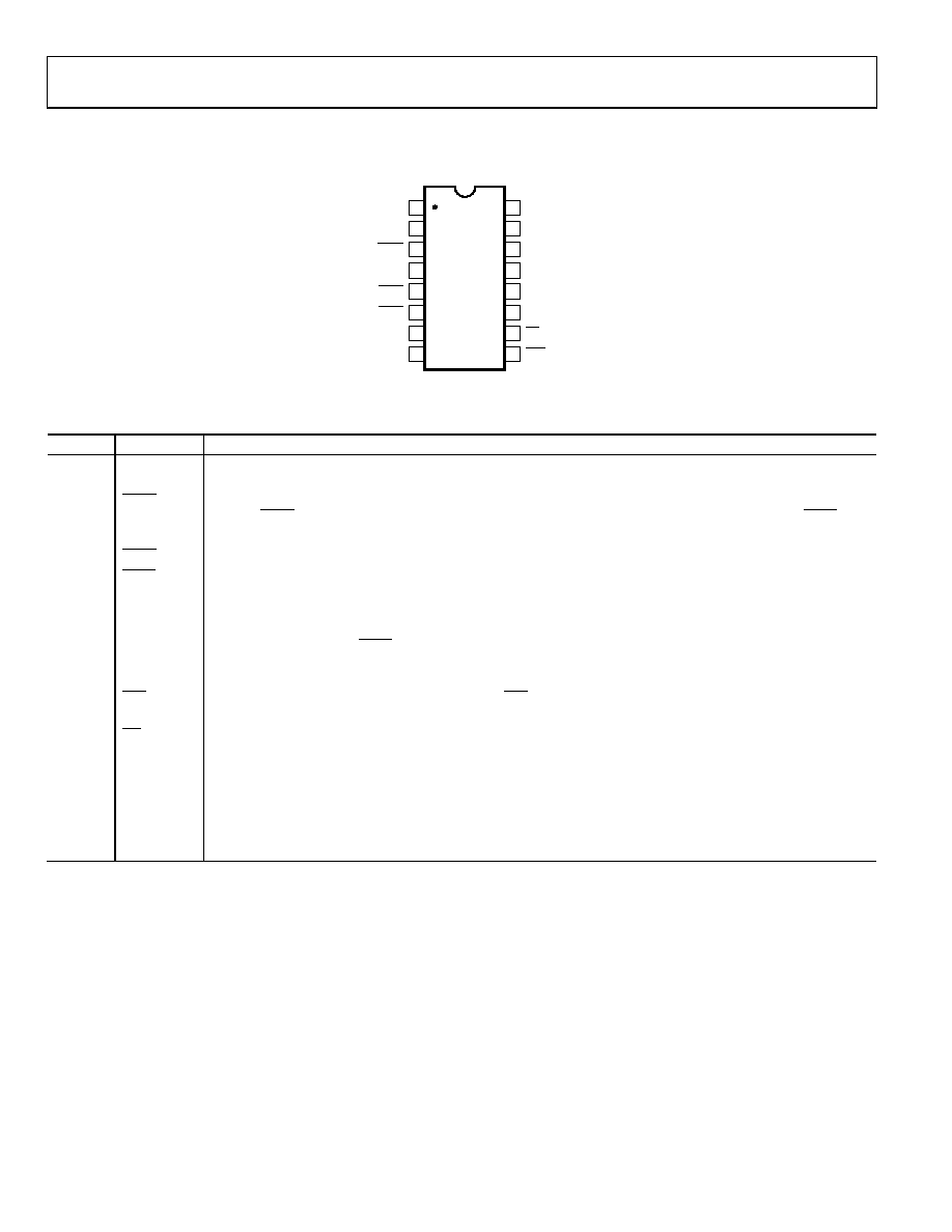
PIN CONFIGURATION AND FUNCTION DESCRIPTIONS
REFAGND
1
REFIN
2
LDAC
3
SDIN
4
SYNC
5
RBEN
6
SCLK
7
SDO
8
VDD
16
VOUT
15
DUTGND
14
VSS
13
NC
12
GND
11
PD
10
CLR
9
AD5530/
AD5531
TOP VIEW
(Not to Scale)
NC = NO CONNECT
0
09
38
-00
4
Figure 4. Pin Configuration
Table 7. Pin Function Descriptions
Pin No.
Mnemonic
Description
1
REFAGND
For bipolar ±10 V output range, this pin should be tied to 0 V.
2
REFIN
This is the voltage reference input for the DAC. Connect to external 5 V reference for specified bipolar ±10 V output.
3
LDAC
Load DAC Logic Input (Active Low). When taken low, the contents of the shift register are transferred to the DAC
register. LDAC can be tied permanently low, enabling the outputs to be updated on the rising edge of SYNC.
4
SDIN
Serial Data Input. This device accepts 16-bit words. Data is clocked into the input register on the falling edge of SCLK.
5
SYNC
Active Low Control Input. Data is clocked into the shift register on the falling edges of SCLK.
6
RBEN
Active Low Readback Enable Function. This function allows the contents of the DAC register to be read. Data
from the DAC register is shifted out on the SDO pin on each rising edge of SCLK.
7
SCLK
Clock Input. Data is clocked into the input register on the falling edge of SCLK.
8
SDO
Serial Data Out. This pin is used to clock out the serial data previously written to the input shift register or can be
used in conjunction with RBEN to read back the data from the DAC register. This is an open drain output; it
should be pulled high with an external pull-up resistor. In standalone mode, SDO should be tied to GND or left
high impedance.
9
CLR
Level Sensitive, Active Low Input. A falling edge of CLR resets VOUT to DUTGND. The contents of the registers
are untouched.
10
PD
This allows the DAC to be put into a power-down state.
11
GND
Ground Reference.
12
NC
Do not connect anything to this pin.
13
VSS
Negative Analog Supply Voltage. 12 V ± 10% or 15 V ± 10%, for specified performance.
14
DUTGND
VOUT is referenced to the voltage applied to this pin.
15
VOUT
DAC Output.
16
VDD
Positive Analog Supply Voltage. 12 V ± 10% or 15 V ± 10%, for specified performance.
相关PDF资料 |
PDF描述 |
|---|---|
| MS3454L20-15S | CONN RCPT 7POS JAM NUT W/SCKT |
| AD5322BRMZ | IC DAC 12BIT DUAL 10MSOP |
| MS27468E23F2P | CONN RCPT 85POS JAM NUT W/PINS |
| VE-262-MW-F3 | CONVERTER MOD DC/DC 15V 100W |
| VI-B01-MY-F4 | CONVERTER MOD DC/DC 12V 50W |
相关代理商/技术参数 |
参数描述 |
|---|---|
| AD5530BRUZ1 | 制造商:AD 制造商全称:Analog Devices 功能描述:Serial Input, Voltage Output 12-/14-Bit Digital-to-Analog Converters |
| AD5530BRUZ-REEL | 功能描述:IC DAC 12BIT SERIAL IN 16TSSOP RoHS:是 类别:集成电路 (IC) >> 数据采集 - 数模转换器 系列:- 产品培训模块:LTC263x 12-, 10-, and 8-Bit VOUT DAC Family 特色产品:LTC2636 - Octal 12-/10-/8-Bit SPI VOUT DACs with 10ppm/°C Reference 标准包装:91 系列:- 设置时间:4µs 位数:10 数据接口:MICROWIRE?,串行,SPI? 转换器数目:8 电压电源:单电源 功率耗散(最大):2.7mW 工作温度:-40°C ~ 85°C 安装类型:表面贴装 封装/外壳:14-WFDFN 裸露焊盘 供应商设备封装:14-DFN-EP(4x3) 包装:管件 输出数目和类型:8 电压,单极 采样率(每秒):* |
| AD5530BRUZ-REEL1 | 制造商:AD 制造商全称:Analog Devices 功能描述:Serial Input, Voltage Output 12-/14-Bit Digital-to-Analog Converters |
| AD5530BRUZ-REEL7 | 功能描述:IC DAC 12BIT SERIAL IN 16TSSOP RoHS:是 类别:集成电路 (IC) >> 数据采集 - 数模转换器 系列:- 产品培训模块:LTC263x 12-, 10-, and 8-Bit VOUT DAC Family 特色产品:LTC2636 - Octal 12-/10-/8-Bit SPI VOUT DACs with 10ppm/°C Reference 标准包装:91 系列:- 设置时间:4µs 位数:10 数据接口:MICROWIRE?,串行,SPI? 转换器数目:8 电压电源:单电源 功率耗散(最大):2.7mW 工作温度:-40°C ~ 85°C 安装类型:表面贴装 封装/外壳:14-WFDFN 裸露焊盘 供应商设备封装:14-DFN-EP(4x3) 包装:管件 输出数目和类型:8 电压,单极 采样率(每秒):* |
| AD5530BRUZ-REEL71 | 制造商:AD 制造商全称:Analog Devices 功能描述:Serial Input, Voltage Output 12-/14-Bit Digital-to-Analog Converters |
发布紧急采购,3分钟左右您将得到回复。