- 您现在的位置:买卖IC网 > PDF目录8655 > AD5555CRUZ-REEL7 (Analog Devices Inc)IC DAC 14BIT DUAL 3WIRE 16-TSSOP PDF资料下载
参数资料
| 型号: | AD5555CRUZ-REEL7 |
| 厂商: | Analog Devices Inc |
| 文件页数: | 2/24页 |
| 文件大小: | 0K |
| 描述: | IC DAC 14BIT DUAL 3WIRE 16-TSSOP |
| 产品培训模块: | Data Converter Fundamentals DAC Architectures |
| 标准包装: | 1,000 |
| 设置时间: | 500ns |
| 位数: | 14 |
| 数据接口: | 串行 |
| 转换器数目: | 2 |
| 电压电源: | 单电源 |
| 功率耗散(最大): | 55µW |
| 工作温度: | -40°C ~ 85°C |
| 安装类型: | 表面贴装 |
| 封装/外壳: | 16-TSSOP(0.173",4.40mm 宽) |
| 供应商设备封装: | 16-TSSOP |
| 包装: | 带卷 (TR) |
| 输出数目和类型: | 2 电流,单极;2 电流,双极 |
| 采样率(每秒): | 2M |
AD5545/AD5555
Data Sheet
Rev. G | Page 10 of 24
SERIAL DATA INTERFACE
The AD5545/AD5555 use a minimum 3-wire (CS, SDI, CLK)
serial data interface for single channel update operation. With
Table 7 as an example (AD5545), users can tie LDAC low
and RS high, and then pull CS low for an 18-bit duration. New
serial data is then clocked into the serial-input register in an 18-
bit data-word format with the MSB bit loaded first. Table 8
defines the truth table for the AD5555. Data is placed on the
SDI pin and clocked into the register on the positive clock edge
of CLK. For the AD5545, only the last 18-bits clocked into the
serial register are interrogated when the CS pin is strobed high,
transferring the serial register data to the DAC register and
updating the output. If the applied microcontroller outputs
serial data in different lengths than the AD5545, such as 8-bit
bytes, three right justified data bytes can be written to the
AD5545. The AD5545 ignores the six MSB and recognizes the
18 LSB as valid data. After loading the serial register, the rising
edge of CS transfers the serial register data to the DAC register
and updates the output; during the CS strobe, the CLK should
not be toggled.
If users want to program each channel separately but update them
simultaneously, program LDAC and RS high initially, then
pull CS low for an 18-bit duration and program DAC A with the
proper address and data bits. CS is then pulled high to latch data
to the DAC A register. At this time, the output is not updated. To
load DAC B data, pull CS low for an 18-bit duration and program
DAC B with the proper address and data, then pull CS high to
latch data to the DAC B register. Finally, pull LDAC low and then
high to update both the DAC A and DAC B outputs
simultaneously.
Table 6 shows that each DAC A and DAC B can be individually
loaded with a new data value. In addition, a common new data
value can be loaded into both DACs simultaneously by setting Bit
A1 = A0 = high. This command enables the parallel combination
of both DACs, with IOUTA and IOUTB tied together, to act as one
DAC with significant improved noise performance.
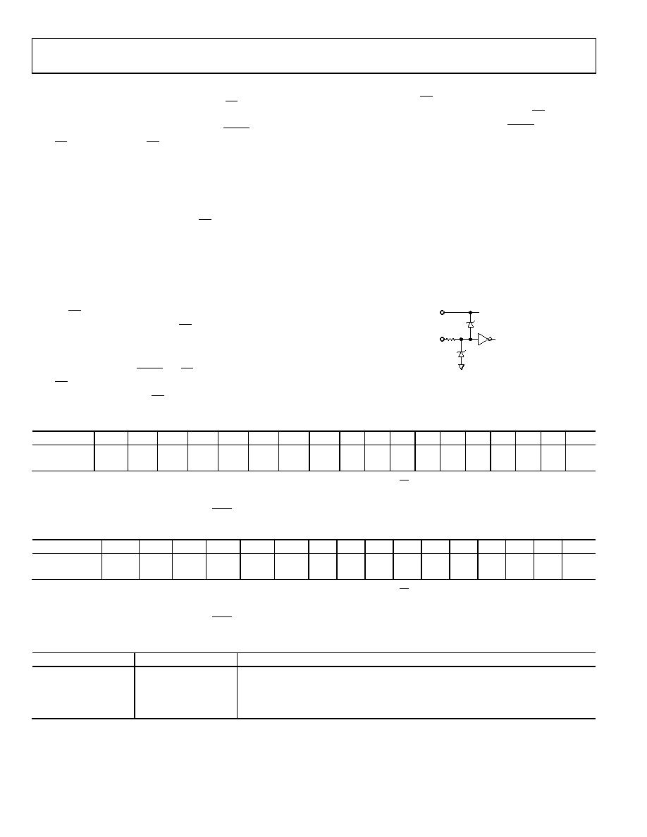
ESD Protection Circuits
All logic input pins contain back-biased ESD protection Zeners
connected to digital ground (DGND) and VDD as shown in
VDD
02918- 0- 007
5k
DGND
DIGITAL
INPUTS
Figure 19. Equivalent ESD Protection Circuits
Table 4. AD5545 Serial Input Register Data Format, Data Is Loaded in the MSB-First Format1
MSB
LSB
Bit Position
B17
B16
B15
B14
B13
B12
B11
B10
B9
B8
B7
B6
B5
B4
B3
B2
B1
B0
Data Word
A1
A0
D15
D14
D13
D12
D11
D10
D9
D8
D7
D6
D5
D4
D3
D2
D1
D0
1
Note that only the last 18 bits of data clocked into the serial register (address + data) are inspected when the CS line’s positive edge
returns to logic high. At this point, an internally generated load strobe transfers the serial register data contents (Bit D15 to Bit D0) to the
decoded DAC input register address determined by Bit A1 and Bit A0. Any extra bits clocked into the AD5545 shift register are ignored; only the last 18 bits clocked in
are used. If double-buffered data is not needed, the LDAC pin can be tied logic low to disable the DAC registers.
Table 5. AD5555 Serial Input Register Data Format, Data Is Loaded in the MSB-First Format1
MSB
LSB
Bit Position
B15
B14
B13
B12
B11
B10
B9
B8
B7
B6
B5
B4
B3
B2
B1
B0
Data Word
A1
A0
D13
D12
D11
D10
D9
D8
D7
D6
D5
D4
D3
D2
D1
D0
1
Note that only the last 16 bits of data clocked into the serial register (address + data) are inspected when the CS line’s positive edge
returns to logic high. At this point, an internally generated load strobe transfers the serial register data contents (Bit D13 to Bit D0) to the
decoded DAC input register address determined by Bit A1 and Bit A0. Any extra bits clocked into the AD5555 shift register are ignored; only the last 16 bits clocked in
are used. If double-buffered data is not needed, the LDAC pin can be tied logic low to disable the DAC registers.
Table 6. Address Decode
A1
A0
DAC Decoded
0
None
0
1
DAC A
1
0
DAC B
1
DAC A and DAC B
相关PDF资料 |
PDF描述 |
|---|---|
| LTC1446LCS8#TRPBF | IC D/A CONV 12BIT R-R DUAL 8SOIC |
| LTC1446LCS8#TR | IC DAC 12BIT DUAL R-R MPWR 8SOIC |
| LTC1450IG#TRPBF | IC D/A CONV 12BIT R-R PAR 24SSOP |
| LTC1450IG#TR | IC DAC 12BIT R-R PAR MPWR 24SSOP |
| LTC1590IS#TR | IC DAC 12BIT MULT DUAL 16SOIC |
相关代理商/技术参数 |
参数描述 |
|---|---|
| AD5556 | 制造商:AD 制造商全称:Analog Devices 功能描述:Dual 8-,10-,12-Bit High Bandwidth Multiplying DACs with Serial Interface |
| AD5556CRU | 功能描述:IC DAC 14BIT PARALL IN 28-TSSOP RoHS:否 类别:集成电路 (IC) >> 数据采集 - 数模转换器 系列:- 标准包装:47 系列:- 设置时间:2µs 位数:14 数据接口:并联 转换器数目:1 电压电源:单电源 功率耗散(最大):55µW 工作温度:-40°C ~ 85°C 安装类型:表面贴装 封装/外壳:28-SSOP(0.209",5.30mm 宽) 供应商设备封装:28-SSOP 包装:管件 输出数目和类型:1 电流,单极;1 电流,双极 采样率(每秒):* |
| AD5556CRU-REEL7 | 功能描述:IC DAC 14BIT PARAL IN 28TSSOP TR RoHS:否 类别:集成电路 (IC) >> 数据采集 - 数模转换器 系列:- 标准包装:47 系列:- 设置时间:2µs 位数:14 数据接口:并联 转换器数目:1 电压电源:单电源 功率耗散(最大):55µW 工作温度:-40°C ~ 85°C 安装类型:表面贴装 封装/外壳:28-SSOP(0.209",5.30mm 宽) 供应商设备封装:28-SSOP 包装:管件 输出数目和类型:1 电流,单极;1 电流,双极 采样率(每秒):* |
| AD5556CRUZ | 功能描述:IC DAC 14BIT PARALL IN 28-TSSOP RoHS:是 类别:集成电路 (IC) >> 数据采集 - 数模转换器 系列:- 产品培训模块:Lead (SnPb) Finish for COTS Obsolescence Mitigation Program 标准包装:50 系列:- 设置时间:4µs 位数:12 数据接口:串行 转换器数目:2 电压电源:单电源 功率耗散(最大):- 工作温度:-40°C ~ 85°C 安装类型:表面贴装 封装/外壳:8-TSSOP,8-MSOP(0.118",3.00mm 宽) 供应商设备封装:8-uMAX 包装:管件 输出数目和类型:2 电压,单极 采样率(每秒):* 产品目录页面:1398 (CN2011-ZH PDF) |
| AD5556CRUZ | 制造商:Analog Devices 功能描述:IC, DAC, 14BIT, TSSOP-28 |
发布紧急采购,3分钟左右您将得到回复。