- 您现在的位置:买卖IC网 > PDF目录8655 > AD5555CRUZ-REEL7 (Analog Devices Inc)IC DAC 14BIT DUAL 3WIRE 16-TSSOP PDF资料下载
参数资料
| 型号: | AD5555CRUZ-REEL7 |
| 厂商: | Analog Devices Inc |
| 文件页数: | 4/24页 |
| 文件大小: | 0K |
| 描述: | IC DAC 14BIT DUAL 3WIRE 16-TSSOP |
| 产品培训模块: | Data Converter Fundamentals DAC Architectures |
| 标准包装: | 1,000 |
| 设置时间: | 500ns |
| 位数: | 14 |
| 数据接口: | 串行 |
| 转换器数目: | 2 |
| 电压电源: | 单电源 |
| 功率耗散(最大): | 55µW |
| 工作温度: | -40°C ~ 85°C |
| 安装类型: | 表面贴装 |
| 封装/外壳: | 16-TSSOP(0.173",4.40mm 宽) |
| 供应商设备封装: | 16-TSSOP |
| 包装: | 带卷 (TR) |
| 输出数目和类型: | 2 电流,单极;2 电流,双极 |
| 采样率(每秒): | 2M |
AD5545/AD5555
Data Sheet
Rev. G | Page 12 of 24
APPLICATIONS INFORMATION
STABILITY
AD5545/AD5555
AD8628
VREF
IOUT
VO
VDD
RFB
U1
U2
C1
GND
02918- 0- 020
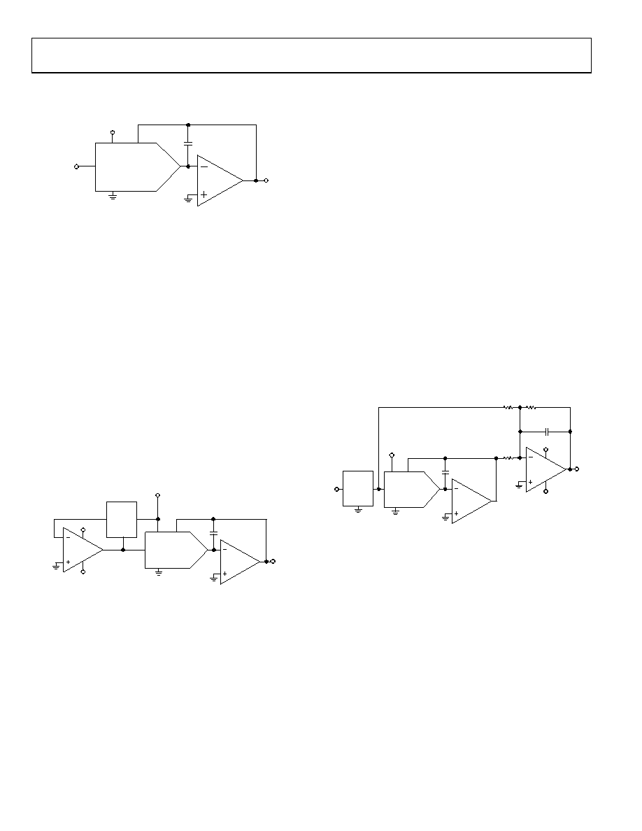
Figure 21. Operational Compensation Capacitor for Gain Peaking
Prevention
In the I-to-V configuration, the IOUT of the DAC and the
inverting node of the op amp must be connected as close as
possible, and proper PCB layout techniques must be employed.
Because every code change corresponds to a step function, gain
peaking may occur if the op amp has limited GBP, and if there
is excessive parasitic capacitance at the inverting node.
An optional compensation capacitor, C1, can be added for
stability as shown in Figure 21. C1 should be found empirically,
but 6 pF is generally more than adequate for the compensation.
POSITIVE VOLTAGE OUTPUT
To achieve the positive voltage output, an applied negative
reference to the input of the DAC is preferred over the output
inversion through an inverting amplifier because of the
resistors’ tolerance errors. To generate a negative reference, the
reference can be level shifted by an op amp such that the VOUT
and GND pins of the reference become the virtual ground and
2.5 V, respectively (see Figure 22).
AD5545/AD5555
1/2
AD8628
1/2
AD8620
ADR03
VREF
IOUT
VOUT VIN
VDD
GND
02918- 0- 021
VO
0 < VO < +2.5
RFB
U2
U1
+5V
V+
–5V
V–
+5V
–2.5V
U3
C1
U4
Figure 22. Positive Voltage Output Configuration
BIPOLAR OUTPUT
The AD5545/AD5555 is inherently a 2-quadrant multiplying
DAC. It can easily be set up for unipolar output operation. The
full-scale output polarity is the inverse of the reference input
voltage.
In some applications, it may be necessary to generate the full
4-quadrant multiplying capability or a bipolar output swing. This
is easily accomplished by using an additional external amplifier,
U4, configured as a summing amplifier (see Figure 23). In this
circuit, the second amplifier, U4, provides a gain of 2, which
increases the output span magnitude to 5 V. Biasing the external
amplifier with a 2.5 V offset from the reference voltage results in a
full 4-quadrant multiplying circuit. The transfer equation of this
circuit shows that both negative and positive output voltages are
created because the input data (D) is incremented from code zero
(VOUT = 2.5 V) to midscale (VOUT = 0 V) to full scale (VOUT =
+2.5 V).
VOUT = (D/32,768 1) × VREF (AD5545)
(3)
VOUT = (D/8192 1) × VREF (AD5555)
(4)
For the AD5545, the external resistance tolerance becomes the
dominant error that users should be aware of.
AD5545/AD5555
1/2
AD8620
1/2
AD8620
ADR03
VREF
IOUT
VOUT VIN
VDD
GND
02918- 0- 022
VO
–2.5 < VO < +2.5
RFB
U2
U3
U1
+5V
V+
–5V
5V
V–
U4
C1
C2
R1
10k
±0.01% 10k±0.01%
5k
±0.01%
R2
R3
Figure 23. Four-Quadrant Multiplying Application Circuit
相关PDF资料 |
PDF描述 |
|---|---|
| LTC1446LCS8#TRPBF | IC D/A CONV 12BIT R-R DUAL 8SOIC |
| LTC1446LCS8#TR | IC DAC 12BIT DUAL R-R MPWR 8SOIC |
| LTC1450IG#TRPBF | IC D/A CONV 12BIT R-R PAR 24SSOP |
| LTC1450IG#TR | IC DAC 12BIT R-R PAR MPWR 24SSOP |
| LTC1590IS#TR | IC DAC 12BIT MULT DUAL 16SOIC |
相关代理商/技术参数 |
参数描述 |
|---|---|
| AD5556 | 制造商:AD 制造商全称:Analog Devices 功能描述:Dual 8-,10-,12-Bit High Bandwidth Multiplying DACs with Serial Interface |
| AD5556CRU | 功能描述:IC DAC 14BIT PARALL IN 28-TSSOP RoHS:否 类别:集成电路 (IC) >> 数据采集 - 数模转换器 系列:- 标准包装:47 系列:- 设置时间:2µs 位数:14 数据接口:并联 转换器数目:1 电压电源:单电源 功率耗散(最大):55µW 工作温度:-40°C ~ 85°C 安装类型:表面贴装 封装/外壳:28-SSOP(0.209",5.30mm 宽) 供应商设备封装:28-SSOP 包装:管件 输出数目和类型:1 电流,单极;1 电流,双极 采样率(每秒):* |
| AD5556CRU-REEL7 | 功能描述:IC DAC 14BIT PARAL IN 28TSSOP TR RoHS:否 类别:集成电路 (IC) >> 数据采集 - 数模转换器 系列:- 标准包装:47 系列:- 设置时间:2µs 位数:14 数据接口:并联 转换器数目:1 电压电源:单电源 功率耗散(最大):55µW 工作温度:-40°C ~ 85°C 安装类型:表面贴装 封装/外壳:28-SSOP(0.209",5.30mm 宽) 供应商设备封装:28-SSOP 包装:管件 输出数目和类型:1 电流,单极;1 电流,双极 采样率(每秒):* |
| AD5556CRUZ | 功能描述:IC DAC 14BIT PARALL IN 28-TSSOP RoHS:是 类别:集成电路 (IC) >> 数据采集 - 数模转换器 系列:- 产品培训模块:Lead (SnPb) Finish for COTS Obsolescence Mitigation Program 标准包装:50 系列:- 设置时间:4µs 位数:12 数据接口:串行 转换器数目:2 电压电源:单电源 功率耗散(最大):- 工作温度:-40°C ~ 85°C 安装类型:表面贴装 封装/外壳:8-TSSOP,8-MSOP(0.118",3.00mm 宽) 供应商设备封装:8-uMAX 包装:管件 输出数目和类型:2 电压,单极 采样率(每秒):* 产品目录页面:1398 (CN2011-ZH PDF) |
| AD5556CRUZ | 制造商:Analog Devices 功能描述:IC, DAC, 14BIT, TSSOP-28 |
发布紧急采购,3分钟左右您将得到回复。