- 您现在的位置:买卖IC网 > PDF目录8568 > AD5570BRS-REEL7 (Analog Devices Inc)IC DAC 16BIT SERIAL IN 16SSOP PDF资料下载
参数资料
| 型号: | AD5570BRS-REEL7 |
| 厂商: | Analog Devices Inc |
| 文件页数: | 13/24页 |
| 文件大小: | 0K |
| 描述: | IC DAC 16BIT SERIAL IN 16SSOP |
| 产品培训模块: | Data Converter Fundamentals DAC Architectures |
| 标准包装: | 500 |
| 设置时间: | 12µs |
| 位数: | 16 |
| 数据接口: | 串行 |
| 转换器数目: | 1 |
| 电压电源: | 双 ± |
| 功率耗散(最大): | 150mW |
| 工作温度: | -40°C ~ 85°C |
| 安装类型: | 表面贴装 |
| 封装/外壳: | 16-SSOP(0.209",5.30mm 宽) |
| 供应商设备封装: | 16-SSOP |
| 包装: | 带卷 (TR) |
| 输出数目和类型: | 1 电压,双极 |
| 采样率(每秒): | 83k |
AD5570
Rev. C | Page 20 of 24
Table 8. Partial List of Precision References Recommended
for Use with the AD5570
Part No.
Initial
Accuracy
(mV max)
Long-Term
Drift
(ppm typ)
Temp Drift
(ppm/
°C max)
0.1 Hz to
10 Hz Noise
(μV p-p typ)
ADR435
±6
30
3
3.4
ADR425
±6
50
3
3.4
±5
50
3
15
ADR395
±6
50
25
5
AD586
±2.5
15
10
4
1 Available in SC70 package.
LAYOUT GUIDELINES
In any circuit where accuracy is important, careful considera-
tion of the power supply and ground return layout helps to
ensure the rated performance. The printed circuit board that
the AD5570 is mounted on is designed so the analog and dig-
ital sections are separated and confined to certain areas of the
board. If the AD5570 is in a system where multiple devices
require an AGND-to-DGND connection, the connection is
made at one point only. The star ground point is established
as close as possible to the device.
The AD5570 has ample supply bypassing of 10 μF in parallel
with 0.1 μF on each supply located as close to the package as
possible, ideally right up against the device. The 10 μF capacitors
are the tantalum bead type. The 0.1 μF capacitor has low effective
series resistance (ESR) and effective series inductance (ESI)
such as the common ceramic types that provide a low imped-
ance path to ground at high frequencies to handle transient
currents due to internal logic switching.
The power supply lines of the AD5570 use as large a trace as pos-
sible to provide low impedance paths and reduce the effects of
glitches on the power supply line. Fast switching signals such as
clocks are shielded with digital ground to avoid radiating noise
to other parts of the board, and are never be run near the refer-
ence inputs. A ground line routed between the SDIN and SCLK
lines reduces crosstalk between them; this is not required on a
multilayer board that has a separate ground plane, but separating
the lines helps. It is essential to minimize noise on the REFIN
line because it couples through to the DAC output.
Avoid crossover of digital and analog signals. Traces on opposite
sides of the board must run at right angles to each other.
This reduces the effects of feed through the board. A micro-
strip technique is by far the best, but not always possible
with a double-sided board. In this technique, the component
side of the board is dedicated to ground plane, while signal
traces are placed on the solder side.
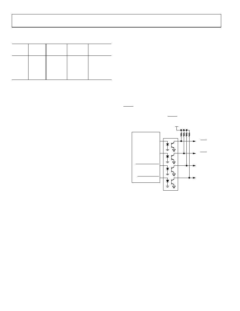
OPTO-ISOLATORS
In many process control applications, it is necessary to provide
an isolation barrier between the controller and the unit being
controlled. Opto-isolators provide voltage isolation in excess of
3 kV. The serial loading structure of the AD5570 makes it ideal
for opto-isolated interfaces, because the number of interface lines
is kept to a minimum. Figure 41 shows a 4-channel isolated inter-
face to the AD5570. To reduce the number of opto-isolators, the
LDAC pin can be tied permanently low if the simultaneous
updating of the DAC is not required. The DAC can then be
updated on the rising edge of SYNC.
VCC
TO SDIN
TO SCLK
TO SYNC
SYNC OUT
SERIAL CLOCK OUT
SERIAL DATA OUT
CONTROLLER
OPTO-COUPLER
TO LDAC
CONTROL OUT
03
76
0-
05
0
Figure 41. Opto-Isolated Interface
相关PDF资料 |
PDF描述 |
|---|---|
| AD5570BRS-REEL | IC DAC 16BIT SERIAL IN 16SSOP |
| AD7847BR | IC DAC 12BIT MULT DUAL 24-SOIC |
| AD810ANZ | IC CURR-FDBK AMP VIDEO LP 8-DIP |
| AD8074ARUZ | IC BUFFER TRPL VIDEO HS 16-TSSOP |
| LT1193IS8 | IC AMP VIDEO DIF ADJ GAIN 8-SOIC |
相关代理商/技术参数 |
参数描述 |
|---|---|
| AD5570BRSZ | 功能描述:IC DAC 16BIT SERIAL IN 16SSOP RoHS:是 类别:集成电路 (IC) >> 数据采集 - 数模转换器 系列:- 标准包装:1 系列:- 设置时间:4.5µs 位数:12 数据接口:串行,SPI? 转换器数目:1 电压电源:单电源 功率耗散(最大):- 工作温度:-40°C ~ 125°C 安装类型:表面贴装 封装/外壳:8-SOIC(0.154",3.90mm 宽) 供应商设备封装:8-SOICN 包装:剪切带 (CT) 输出数目和类型:1 电压,单极;1 电压,双极 采样率(每秒):* 其它名称:MCP4921T-E/SNCTMCP4921T-E/SNRCTMCP4921T-E/SNRCT-ND |
| AD5570BRSZ-REEL | 功能描述:IC DAC 16BIT SERIAL IN 16SSOP RoHS:是 类别:集成电路 (IC) >> 数据采集 - 数模转换器 系列:- 产品培训模块:Data Converter Fundamentals DAC Architectures 标准包装:750 系列:- 设置时间:7µs 位数:16 数据接口:并联 转换器数目:1 电压电源:双 ± 功率耗散(最大):100mW 工作温度:0°C ~ 70°C 安装类型:表面贴装 封装/外壳:28-LCC(J 形引线) 供应商设备封装:28-PLCC(11.51x11.51) 包装:带卷 (TR) 输出数目和类型:1 电压,单极;1 电压,双极 采样率(每秒):143k |
| AD5570BRSZ-REEL7 | 功能描述:IC DAC 16BIT SERIAL IN 16SSOP RoHS:是 类别:集成电路 (IC) >> 数据采集 - 数模转换器 系列:- 产品培训模块:Data Converter Fundamentals DAC Architectures 标准包装:750 系列:- 设置时间:7µs 位数:16 数据接口:并联 转换器数目:1 电压电源:双 ± 功率耗散(最大):100mW 工作温度:0°C ~ 70°C 安装类型:表面贴装 封装/外壳:28-LCC(J 形引线) 供应商设备封装:28-PLCC(11.51x11.51) 包装:带卷 (TR) 输出数目和类型:1 电压,单极;1 电压,双极 采样率(每秒):143k |
| AD5570WRS | 功能描述:IC DAC 16BIT SRL-IN/VOUT 16-SSOP RoHS:否 类别:集成电路 (IC) >> 数据采集 - 数模转换器 系列:- 产品培训模块:Data Converter Fundamentals DAC Architectures 标准包装:750 系列:- 设置时间:7µs 位数:16 数据接口:并联 转换器数目:1 电压电源:双 ± 功率耗散(最大):100mW 工作温度:0°C ~ 70°C 安装类型:表面贴装 封装/外壳:28-LCC(J 形引线) 供应商设备封装:28-PLCC(11.51x11.51) 包装:带卷 (TR) 输出数目和类型:1 电压,单极;1 电压,双极 采样率(每秒):143k |
| AD5570WRS-REEL | 制造商:Analog Devices 功能描述:DAC 1-CH R-2R 16-bit 16-Pin SSOP T/R 制造商:Analog Devices 功能描述:DAC 1CH R-2R 16BIT 16SSOP - Tape and Reel |
发布紧急采购,3分钟左右您将得到回复。