- 您现在的位置:买卖IC网 > PDF目录8568 > AD5570BRS-REEL7 (Analog Devices Inc)IC DAC 16BIT SERIAL IN 16SSOP PDF资料下载
参数资料
| 型号: | AD5570BRS-REEL7 |
| 厂商: | Analog Devices Inc |
| 文件页数: | 9/24页 |
| 文件大小: | 0K |
| 描述: | IC DAC 16BIT SERIAL IN 16SSOP |
| 产品培训模块: | Data Converter Fundamentals DAC Architectures |
| 标准包装: | 500 |
| 设置时间: | 12µs |
| 位数: | 16 |
| 数据接口: | 串行 |
| 转换器数目: | 1 |
| 电压电源: | 双 ± |
| 功率耗散(最大): | 150mW |
| 工作温度: | -40°C ~ 85°C |
| 安装类型: | 表面贴装 |
| 封装/外壳: | 16-SSOP(0.209",5.30mm 宽) |
| 供应商设备封装: | 16-SSOP |
| 包装: | 带卷 (TR) |
| 输出数目和类型: | 1 电压,双极 |
| 采样率(每秒): | 83k |
AD5570
Rev. C | Page 17 of 24
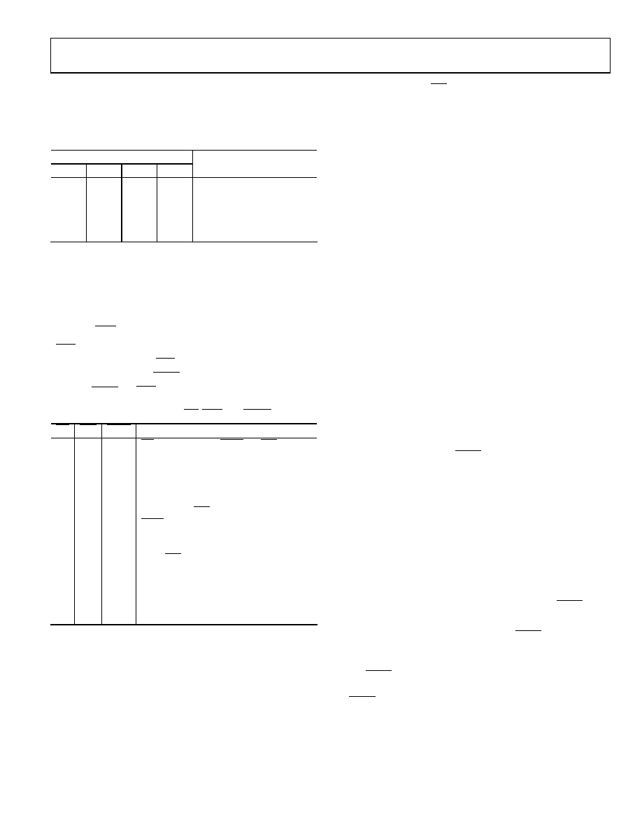
TRANSFER FUNCTION
Table 6 shows the ideal input code to the output voltage rela-
tionship for the AD5570.
Table 6. Binary Code Table
Digital Input
MSB
LSB
Analog Output (VOUT)
1111
+2 VREF × (32,767/32,768)
1000
0000
0001
+2 VREF × (1/32,768)
1000
0000
0 V
0111
1111
2 VREF × (1/32,768)
0000
2 VREF
The output voltage expression is given by
]
65536
/
[
4
2
D
V
REFIN
OUT
×
+
=
where:
D
is the decimal equivalent of the code loaded to the DAC.
VREFIN
is the reference voltage available at the REFIN pin.
CLEAR (CLR)
CLR is an active low digital input that allows the output to be
cleared to 0 V. When the CLR signal is brought back high, the
output stays at 0 V until LDAC is brought low. The relationship
between LDAC and CLR is explained further in
Table 7. Relationships Among PD, CLR, and LDAC
PD
CLR
LDAC
Comments
0
x
PD has priority over LDAC and CLR. The
output remains at 0 V through an internal
20 kΩ resistor. It is still possible to address
both the input register and DAC register
when the AD5570 is in power-down.
1
0
Data is written to the input register and
DAC register. CLR has higher priority over
LDAC; therefore, the output is at 0 V.
1
0
1
Data is written to the input register only.
The output is at 0 V and remains at 0 V
when CLR is taken back high.
1
0
Data is written to the input register and the
DAC register. The output is driven to the
DAC level.
1
Data is written to the input register only.
The output of the DAC register is unchanged.
POWER-DOWN (PD)
The power-down pin allows the user to place the AD5570 into
a power-down mode. In power-down mode, power consump-
tion is at a minimum; the device typically consumes only 16 μA.
POWER-ON RESET
The AD5570 contains a power-on reset circuit that controls the
output during power-up and power-down. This is useful in appli-
cations where the known state of the output of the DAC during
power-up is important. On power-up and power-down, the output
of the DAC and VOUT, is held at AGND.
SERIAL DATA OUTPUT (SDO)
The SDO is the internal shift registers output. For the AD5570,
SDO is an internal pull-down only; an external pull-up resistor
of ~5 kΩ to external logic high is required. SDO pull-down is
disabled when the device is in power-down, thus saving current.
The availability of SDO allows any number of AD5570s to be
daisy-chained together. It also allows for the contents of the DAC
register, or any number of DACs daisy-chained together, to be
read back for diagnostic purposes.
Daisy Chaining
This mode of operation is designed for multi DAC systems,
where several AD5570s can be connected in cascade as shown
in Figure 38. This is done by connecting the control inputs in
parallel and then daisy-chaining the SDIN and SDO I/Os of
each device. An external pull-up resistor of ~5 kΩ on SDO is
required when using the part in daisy-chain mode.
As described earlier, when SYNC goes low, serial data on SDIN
is shifted into the input shift register on the falling edge of SCLK.
If more than 16 clock pulses are applied, the data ripples out of
the shift resister and appears on the SDO line. By connecting
this line to the SDIN input on the next AD5570 in the chain, a
multi DAC interface can be constructed.
One data transfer cycle of 16 SCLK pulses is required for each
DAC in the system. Therefore, the total number of clock cycles
must equal 16 N, where N is the total number of devices in the
chain. The first data transfer cycle written into the chain appears at
the last DAC in the system on the final data transfer cycle.
When the serial transfer to all devices is complete, take SYNC high.
This prevents any further data from being clocked into the devices.
A continuous SCLK source can be used if SYNC is held low
for the correct number of clock cycles. Alternatively, a burst
clock containing the exact number of clock cycles can be used
and SYNC is taken high some time later. The outputs of all the
DACs in the system can be updated simultaneously using the
LDAC signal.
相关PDF资料 |
PDF描述 |
|---|---|
| AD5570BRS-REEL | IC DAC 16BIT SERIAL IN 16SSOP |
| AD7847BR | IC DAC 12BIT MULT DUAL 24-SOIC |
| AD810ANZ | IC CURR-FDBK AMP VIDEO LP 8-DIP |
| AD8074ARUZ | IC BUFFER TRPL VIDEO HS 16-TSSOP |
| LT1193IS8 | IC AMP VIDEO DIF ADJ GAIN 8-SOIC |
相关代理商/技术参数 |
参数描述 |
|---|---|
| AD5570BRSZ | 功能描述:IC DAC 16BIT SERIAL IN 16SSOP RoHS:是 类别:集成电路 (IC) >> 数据采集 - 数模转换器 系列:- 标准包装:1 系列:- 设置时间:4.5µs 位数:12 数据接口:串行,SPI? 转换器数目:1 电压电源:单电源 功率耗散(最大):- 工作温度:-40°C ~ 125°C 安装类型:表面贴装 封装/外壳:8-SOIC(0.154",3.90mm 宽) 供应商设备封装:8-SOICN 包装:剪切带 (CT) 输出数目和类型:1 电压,单极;1 电压,双极 采样率(每秒):* 其它名称:MCP4921T-E/SNCTMCP4921T-E/SNRCTMCP4921T-E/SNRCT-ND |
| AD5570BRSZ-REEL | 功能描述:IC DAC 16BIT SERIAL IN 16SSOP RoHS:是 类别:集成电路 (IC) >> 数据采集 - 数模转换器 系列:- 产品培训模块:Data Converter Fundamentals DAC Architectures 标准包装:750 系列:- 设置时间:7µs 位数:16 数据接口:并联 转换器数目:1 电压电源:双 ± 功率耗散(最大):100mW 工作温度:0°C ~ 70°C 安装类型:表面贴装 封装/外壳:28-LCC(J 形引线) 供应商设备封装:28-PLCC(11.51x11.51) 包装:带卷 (TR) 输出数目和类型:1 电压,单极;1 电压,双极 采样率(每秒):143k |
| AD5570BRSZ-REEL7 | 功能描述:IC DAC 16BIT SERIAL IN 16SSOP RoHS:是 类别:集成电路 (IC) >> 数据采集 - 数模转换器 系列:- 产品培训模块:Data Converter Fundamentals DAC Architectures 标准包装:750 系列:- 设置时间:7µs 位数:16 数据接口:并联 转换器数目:1 电压电源:双 ± 功率耗散(最大):100mW 工作温度:0°C ~ 70°C 安装类型:表面贴装 封装/外壳:28-LCC(J 形引线) 供应商设备封装:28-PLCC(11.51x11.51) 包装:带卷 (TR) 输出数目和类型:1 电压,单极;1 电压,双极 采样率(每秒):143k |
| AD5570WRS | 功能描述:IC DAC 16BIT SRL-IN/VOUT 16-SSOP RoHS:否 类别:集成电路 (IC) >> 数据采集 - 数模转换器 系列:- 产品培训模块:Data Converter Fundamentals DAC Architectures 标准包装:750 系列:- 设置时间:7µs 位数:16 数据接口:并联 转换器数目:1 电压电源:双 ± 功率耗散(最大):100mW 工作温度:0°C ~ 70°C 安装类型:表面贴装 封装/外壳:28-LCC(J 形引线) 供应商设备封装:28-PLCC(11.51x11.51) 包装:带卷 (TR) 输出数目和类型:1 电压,单极;1 电压,双极 采样率(每秒):143k |
| AD5570WRS-REEL | 制造商:Analog Devices 功能描述:DAC 1-CH R-2R 16-bit 16-Pin SSOP T/R 制造商:Analog Devices 功能描述:DAC 1CH R-2R 16BIT 16SSOP - Tape and Reel |
发布紧急采购,3分钟左右您将得到回复。