参数资料
| 型号: | AD5623RBRMZ-5 |
| 厂商: | Analog Devices Inc |
| 文件页数: | 13/32页 |
| 文件大小: | 0K |
| 描述: | IC DAC NANO 12BIT DUAL 10-MSOP |
| 产品培训模块: | Data Converter Fundamentals DAC Architectures |
| 标准包装: | 50 |
| 系列: | nanoDAC™ |
| 设置时间: | 3µs |
| 位数: | 12 |
| 数据接口: | 串行 |
| 转换器数目: | 2 |
| 电压电源: | 单电源 |
| 功率耗散(最大): | 5mW |
| 工作温度: | -40°C ~ 105°C |
| 安装类型: | 表面贴装 |
| 封装/外壳: | 10-TFSOP,10-MSOP(0.118",3.00mm 宽) |
| 供应商设备封装: | 10-MSOP |
| 包装: | 管件 |
| 输出数目和类型: | 2 电压,单极;2 电压,双极 |
| 采样率(每秒): | 287k |
| 产品目录页面: | 783 (CN2011-ZH PDF) |
第1页第2页第3页第4页第5页第6页第7页第8页第9页第10页第11页第12页当前第13页第14页第15页第16页第17页第18页第19页第20页第21页第22页第23页第24页第25页第26页第27页第28页第29页第30页第31页第32页
AD5623R/AD5643R/AD5663R
Data Sheet
Rev. E | Page 20 of 32
THEORY OF OPERATION
DIGITAL-TO-ANALOG SECTION
The AD5623R/AD5643R/AD5663R DAC is fabricated on
a CMOS process. The architecture consists of a string DAC
followed by an output buffer amplifier. Figure 49 shows a block
diagram of the DAC architecture.
DAC
REGISTER
RESISTOR
STRING
REF (+)
VDD
GND
REF (–)
VOUT
OUTPUT
AMPLIFIER
(GAIN = +2)
0
585
8-
0
32
Figure 49. DAC Architecture
Because the input coding to the DAC is straight binary, the ideal
output voltage when using an external reference is given by
N
REFIN
OUT
D
V
2
The ideal output voltage when using the internal reference is
given by
N
REFOUT
OUT
D
V
2
where:
D
is the decimal equivalent of the binary code that is loaded to
the DAC register:
0 to 4095 for AD5623R (12-bit)
0 to 16,383 for AD5643R (14-bit)
0 to 65,535 for AD5663R (16-bit)
N
is the DAC resolution.
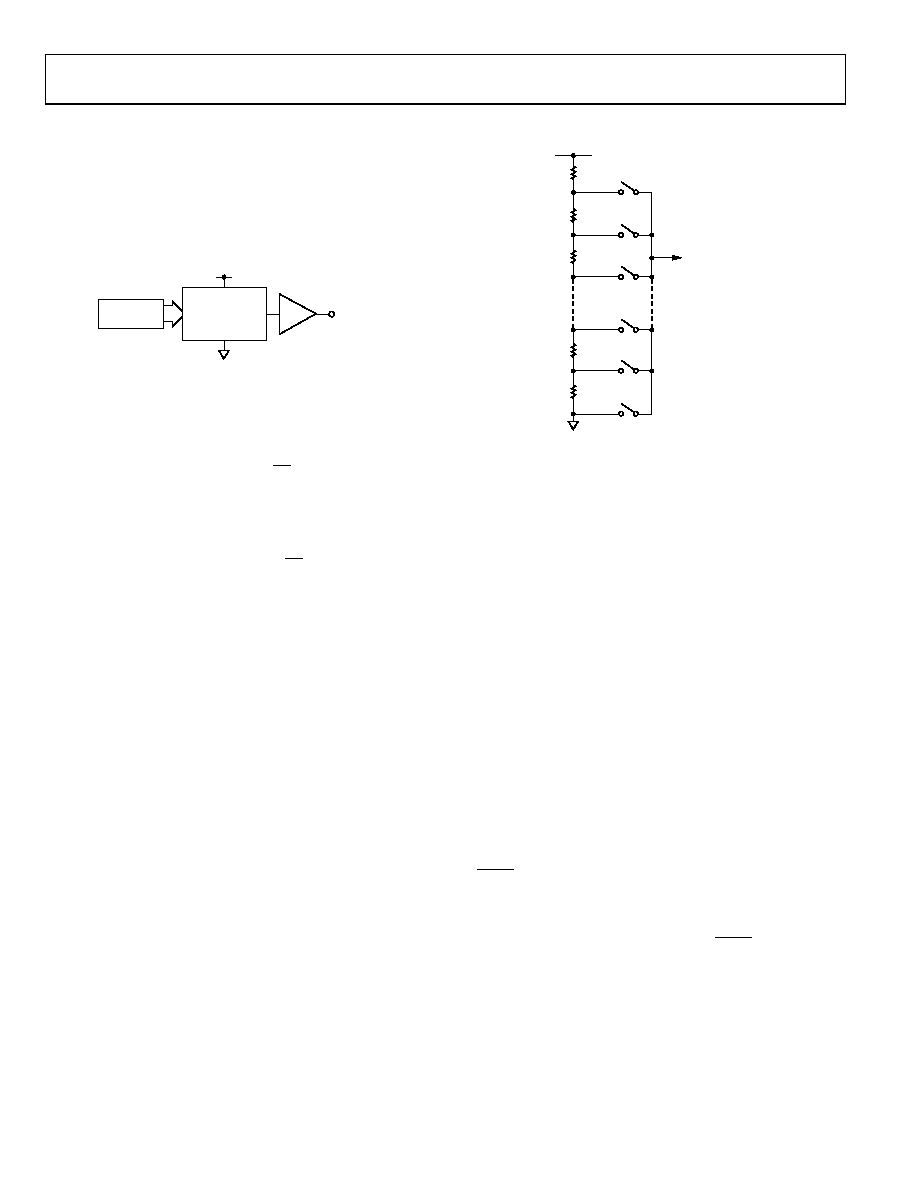
RESISTOR STRING
The resistor string section is shown in Figure 50. It is simply a
string of resistors, each of Value R. The code loaded to the DAC
register determines at which node on the string the voltage is
tapped off to be fed into the output amplifier. The voltage is
tapped off by closing one of the switches connecting the string
to the amplifier. Because it is a string of resistors, it is guaranteed
monotonic.
OUTPUT AMPLIFIER
The output buffer amplifier can generate rail-to-rail voltages on
its output, which gives an output range of 0 V to VDD. It can drive
a load of 2 kΩ in parallel with 1000 pF to GND. The source and
sink capabilities of the output amplifier can be seen in Figure 31.
The slew rate is 1.8 V/μs with a 1/4 to 3/4 full-scale settling time
of 10 μs.
R
TO OUTPUT
AMPLIFIER
0
58
-0
33
Figure 50. Resistor String
INTERNAL REFERENCE
The AD5623R/AD5643R/AD5663R on-chip reference is off at
power-up and is enabled via a write to a control register. See the
Internal Reference Setup section for details.
The AD56x3R-3 has a 1.25 V, 5 ppm/°C reference, giving a full-
scale output of 2.5 V. The AD56x3R-5 has a 2.5 V, 5 ppm/°C
reference, giving a full-scale output of 5 V. The internal refer-
ence associated with each part is available at the VREFOUT pin.
A buffer is required if the reference output is used to drive
external loads. When using the internal reference, it is
recommended that a 100 nF capacitor be placed between
reference output and GND for reference stability.
EXTERNAL REFERENCE
The VREFIN pins on the AD56x3R-3 and the AD56x3R-5 allows
the use of an external reference if the application requires it.
The on-chip reference is off at power-up, and this is the default
condition. The AD56x3R-3 and the AD56x3R-5 can be operated
from a single 2.7 V to 5.5 V supply.
SERIAL INTERFACE
The AD5623R/AD5643R/AD5663R have a 3-wire serial interface
(SYNC, SCLK, and DIN) that is compatible with SPI, QSPI, and
MICROWIRE interface standards, as well as with most DSPs.
See Figure 2 for a timing diagram of a typical write sequence.
The write sequence begins by bringing the SYNC line low. Data
from the DIN line is clocked into the 24-bit shift register on the
falling edge of SCLK. The serial clock frequency can be as high
as 50 MHz, making the AD5623R/AD5643R/AD5663R compatible
with high speed DSPs. On the 24th falling clock edge, the last
data bit is clocked in and the programmed function is executed,
for example, a change in DAC register contents and/or a change
in the mode of operation.
相关PDF资料 |
PDF描述 |
|---|---|
| MS3454W14S-7PW | CONN RCPT 3POS JAM NUT W/PINS |
| AD5312BRMZ | IC DAC 10BIT DUAL R-R 10-MSOP |
| VI-201-MY-F1 | CONVERTER MOD DC/DC 12V 50W |
| VI-J5R-MZ-F3 | CONVERTER MOD DC/DC 7.5V 25W |
| VI-J5R-MZ-F2 | CONVERTER MOD DC/DC 7.5V 25W |
相关代理商/技术参数 |
参数描述 |
|---|---|
| AD5623RBRMZ-5REEL7 | 功能描述:IC DAC NANO 12BIT DUAL 10-MSOP RoHS:是 类别:集成电路 (IC) >> 数据采集 - 数模转换器 系列:nanoDAC™ 产品培训模块:LTC263x 12-, 10-, and 8-Bit VOUT DAC Family 特色产品:LTC2636 - Octal 12-/10-/8-Bit SPI VOUT DACs with 10ppm/°C Reference 标准包装:91 系列:- 设置时间:4µs 位数:10 数据接口:MICROWIRE?,串行,SPI? 转换器数目:8 电压电源:单电源 功率耗散(最大):2.7mW 工作温度:-40°C ~ 85°C 安装类型:表面贴装 封装/外壳:14-WFDFN 裸露焊盘 供应商设备封装:14-DFN-EP(4x3) 包装:管件 输出数目和类型:8 电压,单极 采样率(每秒):* |
| AD5624 | 制造商:AD 制造商全称:Analog Devices 功能描述:2.7 V to 5.5 V, 450 レA, Rail-to-Rail Output, Quad, 12-/16-Bit nanoDACs |
| AD5624BCPZ-250RL7 | 制造商:AD 制造商全称:Analog Devices 功能描述:2.7 V to 5.5 V, 450 レA, Rail-to-Rail Output, Quad, 12-/16-Bit nanoDACs |
| AD5624BCPZ-R2 | 功能描述:IC DAC NANO 12BIT QUAD 10-LFCSP RoHS:是 类别:集成电路 (IC) >> 数据采集 - 数模转换器 系列:nanoDAC™ 标准包装:47 系列:- 设置时间:2µs 位数:14 数据接口:并联 转换器数目:1 电压电源:单电源 功率耗散(最大):55µW 工作温度:-40°C ~ 85°C 安装类型:表面贴装 封装/外壳:28-SSOP(0.209",5.30mm 宽) 供应商设备封装:28-SSOP 包装:管件 输出数目和类型:1 电流,单极;1 电流,双极 采样率(每秒):* |
| AD5624BCPZ-REEL7 | 功能描述:IC DAC NANO 12BIT QUAD 10-LFCSP RoHS:是 类别:集成电路 (IC) >> 数据采集 - 数模转换器 系列:nanoDAC™ 产品培训模块:LTC263x 12-, 10-, and 8-Bit VOUT DAC Family 特色产品:LTC2636 - Octal 12-/10-/8-Bit SPI VOUT DACs with 10ppm/°C Reference 标准包装:91 系列:- 设置时间:4µs 位数:10 数据接口:MICROWIRE?,串行,SPI? 转换器数目:8 电压电源:单电源 功率耗散(最大):2.7mW 工作温度:-40°C ~ 85°C 安装类型:表面贴装 封装/外壳:14-WFDFN 裸露焊盘 供应商设备封装:14-DFN-EP(4x3) 包装:管件 输出数目和类型:8 电压,单极 采样率(每秒):* |
发布紧急采购,3分钟左右您将得到回复。