参数资料
| 型号: | AD5623RBRMZ-5 |
| 厂商: | Analog Devices Inc |
| 文件页数: | 14/32页 |
| 文件大小: | 0K |
| 描述: | IC DAC NANO 12BIT DUAL 10-MSOP |
| 产品培训模块: | Data Converter Fundamentals DAC Architectures |
| 标准包装: | 50 |
| 系列: | nanoDAC™ |
| 设置时间: | 3µs |
| 位数: | 12 |
| 数据接口: | 串行 |
| 转换器数目: | 2 |
| 电压电源: | 单电源 |
| 功率耗散(最大): | 5mW |
| 工作温度: | -40°C ~ 105°C |
| 安装类型: | 表面贴装 |
| 封装/外壳: | 10-TFSOP,10-MSOP(0.118",3.00mm 宽) |
| 供应商设备封装: | 10-MSOP |
| 包装: | 管件 |
| 输出数目和类型: | 2 电压,单极;2 电压,双极 |
| 采样率(每秒): | 287k |
| 产品目录页面: | 783 (CN2011-ZH PDF) |
第1页第2页第3页第4页第5页第6页第7页第8页第9页第10页第11页第12页第13页当前第14页第15页第16页第17页第18页第19页第20页第21页第22页第23页第24页第25页第26页第27页第28页第29页第30页第31页第32页
Data Sheet
AD5623R/AD5643R/AD5663R
Rev. E | Page 21 of 32
At this stage, the SYNC line can be kept low or be brought high.
In either case, it must be brought high for a minimum of 15 ns
before the next write sequence, so that a falling edge of SYNC
can initiate the next write sequence.
Because the SYNC buffer draws more current when VIN = 2 V
than it does when VIN = 0.8 V, SYNC should be idled low between
write sequences for even lower power operation. As mentioned
previously, it must, however, be brought high again just before
the next write sequence.
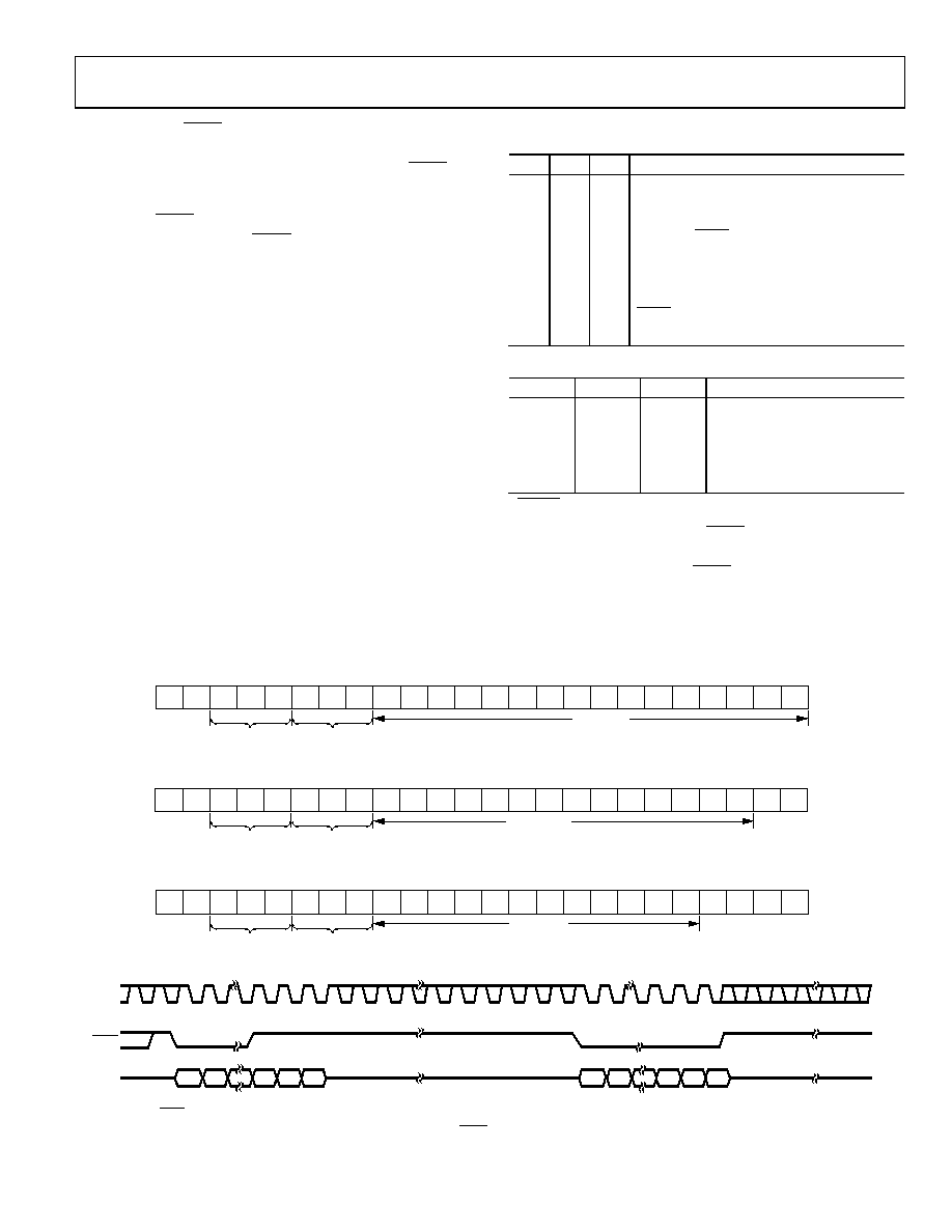
INPUT SHIFT REGISTER
The input shift register is 24 bits wide (see Figure 52). The first
two bits are don’t cares. The next three are Command Bit C2 to
Command Bit C0 (see Table 8), followed by the 3-bit DAC
Address A2 to DAC Address A0 (see Table 9), and, finally, the
16-, 14-, and 12-bit data-word.
The data-word comprises the 16-, 14-, and 12-bit input codes,
followed by zero, two, or four don’t care bits, for the AD5663R,
AD5643R, and AD5623R, respectively (see Figure 51, Figure 52,
and Figure 53). The data bits are transferred to the DAC register
on the 24th falling edge of SCLK.
Table 8. Command Definition
C2
C1
C0
Command
0
Write to Input Register n
0
1
Update DAC Register n
0
1
0
Write to Input Register n, update all
(software LDAC)
0
1
Write to and update DAC Channel n
1
0
Power down DAC (power up)
1
0
1
Reset
1
0
LDAC register setup
1
Internal reference setup (on/off)
Table 9. Address Command
A2
A1
A0
ADDRESS (n)
0
DAC A
0
1
DAC B
0
1
0
Reserved
0
1
Reserved
1
All DACs
SYNC INTERRUPT
In a normal write sequence, the SYNC line is kept low for at
least 24 falling edges of SCLK, and the DAC is updated on the
24th falling edge. However, if SYNC is brought high before the
24th falling edge, this acts as an interrupt to the write sequence.
The shift register is reset, and the write sequence is seen as
invalid. Neither an update of the DAC register contents nor a
change in the operating mode occurs (see Figure 54).
X
C2
C1
C0
A2
A1
A0
D15
D14
D13
D12
D11
D10
D9
D8
D7
D6
D5
D4
D3
D2
D1
D0
DB23 (MSB)
DB0 (LSB)
COMMAND BITS
ADDRESS BITS
DATA BITS
05858-
034
Figure 51. AD5663R Input Shift Register Contents
X
C2
C1
C0
A2
A1
A0
X
D11
D10
D13
D12
D9
D8
D7
D6
D5
D4
D3
D2
D1
D0
DB23 (MSB)
DB0 (LSB)
COMMAND BITS
ADDRESS BITS
DATA BITS
05858-
071
Figure 52. AD5643R Input Shift Register Contents
X
C2
C1
C0
A2
A1
A0
X
D11
D10
D9
D8
D7
D6
D5
D4
D3
D2
D1
D0
DB23 (MSB)
DB0 (LSB)
COMMAND BITS
ADDRESS BITS
DATA BITS
05858-
072
Figure 53. AD5623R Input Shift Register Contents
DIN
DB23
DB0
VALID WRITE SEQUENCE, OUTPUT UPDATES
ON THE 24TH FALLING EDGE
SYNC
SCLK
INVALID WRITE SEQUENCE:
SYNC HIGH BEFORE 24TH FALLING EDGE
05858-
035
Figure 54. SYNC Interrupt Facility
相关PDF资料 |
PDF描述 |
|---|---|
| MS3454W14S-7PW | CONN RCPT 3POS JAM NUT W/PINS |
| AD5312BRMZ | IC DAC 10BIT DUAL R-R 10-MSOP |
| VI-201-MY-F1 | CONVERTER MOD DC/DC 12V 50W |
| VI-J5R-MZ-F3 | CONVERTER MOD DC/DC 7.5V 25W |
| VI-J5R-MZ-F2 | CONVERTER MOD DC/DC 7.5V 25W |
相关代理商/技术参数 |
参数描述 |
|---|---|
| AD5623RBRMZ-5REEL7 | 功能描述:IC DAC NANO 12BIT DUAL 10-MSOP RoHS:是 类别:集成电路 (IC) >> 数据采集 - 数模转换器 系列:nanoDAC™ 产品培训模块:LTC263x 12-, 10-, and 8-Bit VOUT DAC Family 特色产品:LTC2636 - Octal 12-/10-/8-Bit SPI VOUT DACs with 10ppm/°C Reference 标准包装:91 系列:- 设置时间:4µs 位数:10 数据接口:MICROWIRE?,串行,SPI? 转换器数目:8 电压电源:单电源 功率耗散(最大):2.7mW 工作温度:-40°C ~ 85°C 安装类型:表面贴装 封装/外壳:14-WFDFN 裸露焊盘 供应商设备封装:14-DFN-EP(4x3) 包装:管件 输出数目和类型:8 电压,单极 采样率(每秒):* |
| AD5624 | 制造商:AD 制造商全称:Analog Devices 功能描述:2.7 V to 5.5 V, 450 レA, Rail-to-Rail Output, Quad, 12-/16-Bit nanoDACs |
| AD5624BCPZ-250RL7 | 制造商:AD 制造商全称:Analog Devices 功能描述:2.7 V to 5.5 V, 450 レA, Rail-to-Rail Output, Quad, 12-/16-Bit nanoDACs |
| AD5624BCPZ-R2 | 功能描述:IC DAC NANO 12BIT QUAD 10-LFCSP RoHS:是 类别:集成电路 (IC) >> 数据采集 - 数模转换器 系列:nanoDAC™ 标准包装:47 系列:- 设置时间:2µs 位数:14 数据接口:并联 转换器数目:1 电压电源:单电源 功率耗散(最大):55µW 工作温度:-40°C ~ 85°C 安装类型:表面贴装 封装/外壳:28-SSOP(0.209",5.30mm 宽) 供应商设备封装:28-SSOP 包装:管件 输出数目和类型:1 电流,单极;1 电流,双极 采样率(每秒):* |
| AD5624BCPZ-REEL7 | 功能描述:IC DAC NANO 12BIT QUAD 10-LFCSP RoHS:是 类别:集成电路 (IC) >> 数据采集 - 数模转换器 系列:nanoDAC™ 产品培训模块:LTC263x 12-, 10-, and 8-Bit VOUT DAC Family 特色产品:LTC2636 - Octal 12-/10-/8-Bit SPI VOUT DACs with 10ppm/°C Reference 标准包装:91 系列:- 设置时间:4µs 位数:10 数据接口:MICROWIRE?,串行,SPI? 转换器数目:8 电压电源:单电源 功率耗散(最大):2.7mW 工作温度:-40°C ~ 85°C 安装类型:表面贴装 封装/外壳:14-WFDFN 裸露焊盘 供应商设备封装:14-DFN-EP(4x3) 包装:管件 输出数目和类型:8 电压,单极 采样率(每秒):* |
发布紧急采购,3分钟左右您将得到回复。