参数资料
| 型号: | AD5626BRMZ-REEL7 |
| 厂商: | Analog Devices Inc |
| 文件页数: | 5/20页 |
| 文件大小: | 0K |
| 描述: | IC DAC NANO 12BIT 8-MSOP |
| 产品培训模块: | Data Converter Fundamentals DAC Architectures |
| 标准包装: | 1 |
| 系列: | nanoDAC™ |
| 设置时间: | 16µs |
| 位数: | 12 |
| 数据接口: | 串行 |
| 转换器数目: | 1 |
| 电压电源: | 单电源 |
| 功率耗散(最大): | 12.5mW |
| 工作温度: | -40°C ~ 85°C |
| 安装类型: | 表面贴装 |
| 封装/外壳: | 8-TSSOP,8-MSOP(0.118",3.00mm 宽) |
| 供应商设备封装: | 8-MSOP |
| 包装: | 标准包装 |
| 输出数目和类型: | 1 电压,单极;1 电压,双极 |
| 采样率(每秒): | * |
| 其它名称: | AD5626BRMZ-REEL7DKR |
AD5626
Rev. A | Page 13 of 20
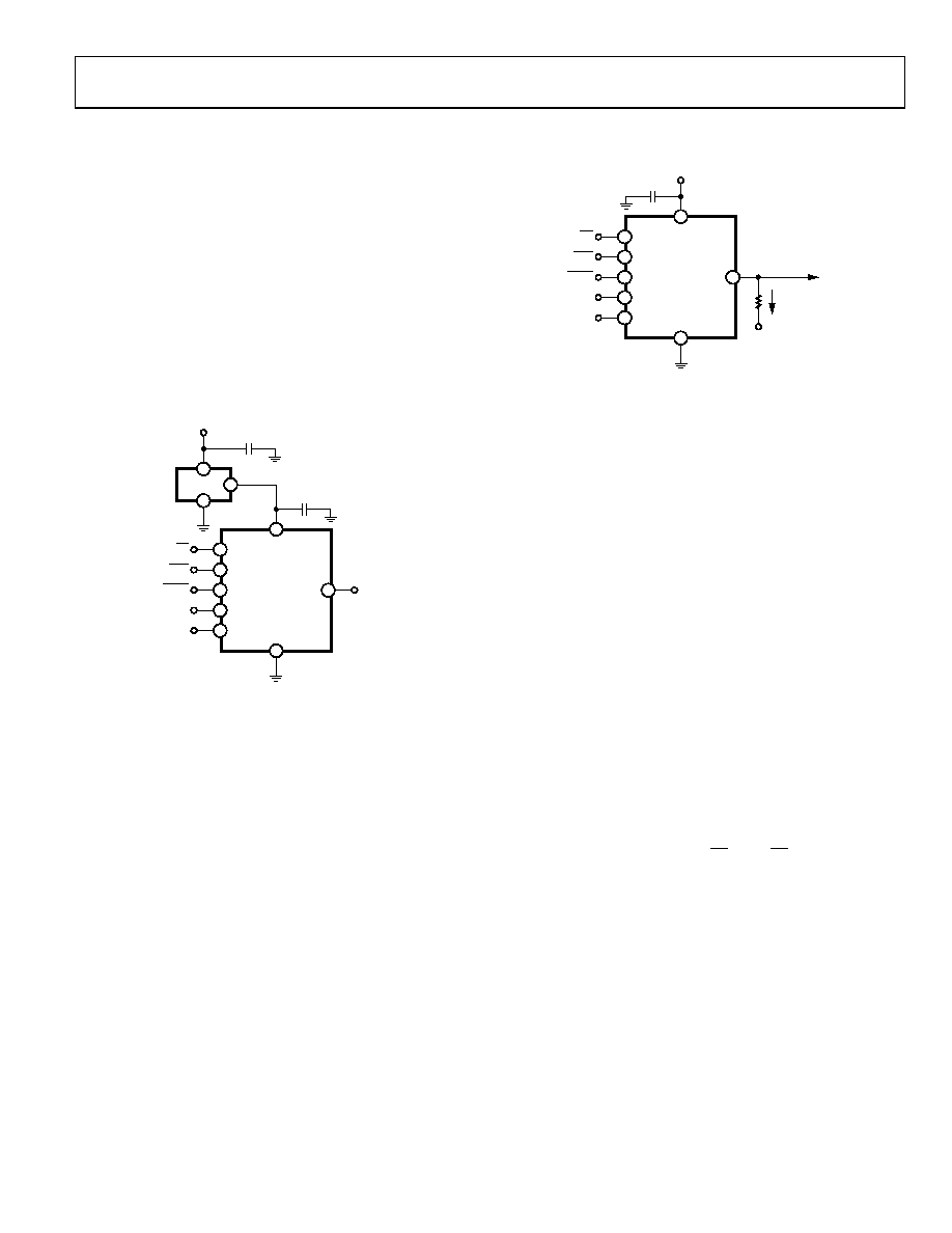
OPERATING THE AD5626 ON 12 V OR 15 V
SUPPLIES ONLY
Although the AD5626 has been specified to operate on a single,
5 V supply, a single 5 V supply may not be available in many
applications. Because the AD5626 consumes no more than 2.5 mA
maximum, an integrated voltage reference, such as the ADR02,
can be used as the 5 V supply for the AD5626. See Figure 28 for
the circuit configuration. Notice that the output voltage of the
reference requires no trimming because of the excellent load
regulation and tight initial output voltage tolerance of the ADR02.
Although the maximum supply current of the AD5626 is 2.5 mA,
local bypassing of the ADR02 output with at least 0.1 μF at the
DAC voltage supply pin is recommended to prevent the internal
digital circuits of the DAC from affecting the internal voltage
reference of the DAC.
0
675
7-
0
28
CS
CLR
SCLK
LDAC
SDIN
2
8
6
5
3
4
1
7
VDD
GND
AD5626
0.1F
VOUT
12V OR 15V
1F
ADR02
2
4
6
Figure 28. Operating the AD5626 on 12 V or 15 V Supplies Using an
ADR02 Voltage Reference
MEASURING OFFSET ERROR
One of the most commonly specified endpoint errors associated
with real world nonideal DACs is offset error. In most DAC
testing, the offset error is measured by applying the zero-scale
code and measuring the output deviation from 0 V.
There are some DACs where offset errors are present but not
observable at the zero scale because of other circuit limitations
(for example, zero coinciding with single-supply ground). In
these DACs, nonzero output at zero code cannot be read as the
offset error. In the AD5626, for example, the zero-scale error is
specified to be ±3 LSBs. Because zero scale coincides with zero
volt, it is not possible to measure negative offset error.
0
67
57
-02
9
CS
CLR
SCLK
V–
LDAC
SDIN
2
8
6
5
3
4
VOUT
1
7
VDD
GND
AD5626
0.1F
5V
200A, MAX
R
VOUT
SET CODE = 0x000 AND MEASURE VOUT
Figure 29. Measuring Zero-Scale or Offset Error
By adding a pull-down resistor from the output of the AD5626
to a negative supply as shown in Figure 29, offset errors can be
read at zero code. This configuration forces the output P-channel
MOSFET to source current to the negative supply thereby allowing
the designer to determine in which direction the offset error
appears. The value of the resistor should be such that, at zero
code, current through the resistor is 200 μA, maximum.
BIPOLAR OUTPUT OPERATION
Although the AD5626 has been designed for single-supply
operation, bipolar operation is achievable using the circuit
illustrated in Figure 30. The circuit uses a single-supply, rail-
to-rail OP295 op amp and the REF03 to generate the 2.5 V
reference required to level shift the DAC output voltage.
Note that the 2.5 V reference is generated without the use of
precision resistors. The circuit configuration provides an output
voltage in the range of 5 V ≤ VOUT ≤ +5 V and is coded in comple-
mentary offset binary. Although each DAC LSB corresponds to
1 mV, each output LSB has been scaled to 2.44 mV. Table 7 lists
the relationship between the digital codes and output voltage.
The transfer function of the circuit is given by
R2
R4
R1
R4
Code
Digital
V
O
×
+
×
=
5
.
2
mV
1
and, for the circuit values shown, becomes
VO = 2.44 mV × Digital Code + 5 V
相关PDF资料 |
PDF描述 |
|---|---|
| AD5662BRM-1 | IC DAC 16BIT BUFF V-OUT 8-MSOP |
| AD5663RBCPZ-3R2 | IC DAC NANO 16BIT DUAL 10-LFCSP |
| AD5664BCPZ-R2 | IC DAC NANO 16BIT QUAD 10-LFCSP |
| AD5667RBRMZ-2 | IC DAC NANO 16BIT DUAL 10-MSOP |
| AD5669RBRUZ-2 | IC DAC 16BIT I2C/SRL 16TSSOP |
相关代理商/技术参数 |
参数描述 |
|---|---|
| AD5627 | 制造商:AD 制造商全称:Analog Devices 功能描述:Dual, 12-/14-/16-Bit nanoDACs with 5ppm/C On-Chip Ref, I2C Interface |
| AD5627BCPZ-250RL7 | 制造商:AD 制造商全称:Analog Devices 功能描述:Dual, 12-/14-/16-Bit nanoDACs with 5ppm/C On-Chip Ref, I2C Interface |
| AD5627BCPZ-R2 | 功能描述:IC DAC 12BIT DUAL 10-LFCSP RoHS:是 类别:集成电路 (IC) >> 数据采集 - 数模转换器 系列:nanoDAC™ 产品培训模块:LTC263x 12-, 10-, and 8-Bit VOUT DAC Family 特色产品:LTC2636 - Octal 12-/10-/8-Bit SPI VOUT DACs with 10ppm/°C Reference 标准包装:91 系列:- 设置时间:4µs 位数:10 数据接口:MICROWIRE?,串行,SPI? 转换器数目:8 电压电源:单电源 功率耗散(最大):2.7mW 工作温度:-40°C ~ 85°C 安装类型:表面贴装 封装/外壳:14-WFDFN 裸露焊盘 供应商设备封装:14-DFN-EP(4x3) 包装:管件 输出数目和类型:8 电压,单极 采样率(每秒):* |
| AD5627BCPZ-REEL7 | 功能描述:IC DAC NANO 12BIT DUAL 10-LFCSP RoHS:是 类别:集成电路 (IC) >> 数据采集 - 数模转换器 系列:nanoDAC™ 产品培训模块:Data Converter Fundamentals DAC Architectures 设计资源:Unipolar, Precision DC Digital-to-Analog Conversion using AD5450/1/2/3 8-14-Bit DACs (CN0052) Precision, Bipolar, Configuration for AD5450/1/2/3 8-14bit Multiplying DACs (CN0053) AC Signal Processing Using AD5450/1/2/3 Current Output DACs (CN0054) Programmable Gain Element Using AD5450/1/2/3 Current Output DAC Family (CN0055) Single Supply Low Noise LED Current Source Driver Using a Current Output DAC in the Reverse Mode (CN0139) 标准包装:10,000 系列:- 设置时间:- 位数:12 数据接口:DSP,MICROWIRE?,QSPI?,串行,SPI? 转换器数目:1 电压电源:单电源 功率耗散(最大):- 工作温度:-40°C ~ 125°C 安装类型:表面贴装 封装/外壳:SOT-23-8 薄型,TSOT-23-8 供应商设备封装:TSOT-23-8 包装:带卷 (TR) 输出数目和类型:1 电流,单极;1 电流,双极 采样率(每秒):2.7M |
| AD5627BRMZ | 功能描述:IC DAC NANO 12BIT DUAL 10-MSOP RoHS:是 类别:集成电路 (IC) >> 数据采集 - 数模转换器 系列:nanoDAC™ 产品培训模块:Lead (SnPb) Finish for COTS Obsolescence Mitigation Program 标准包装:50 系列:- 设置时间:4µs 位数:12 数据接口:串行 转换器数目:2 电压电源:单电源 功率耗散(最大):- 工作温度:-40°C ~ 85°C 安装类型:表面贴装 封装/外壳:8-TSSOP,8-MSOP(0.118",3.00mm 宽) 供应商设备封装:8-uMAX 包装:管件 输出数目和类型:2 电压,单极 采样率(每秒):* 产品目录页面:1398 (CN2011-ZH PDF) |
发布紧急采购,3分钟左右您将得到回复。