- 您现在的位置:买卖IC网 > PDF目录8630 > AD5629RBCPZ-2-RL7 (Analog Devices Inc)IC DAC 12BIT I2C/SRL 16LFCSP-WQ PDF资料下载
参数资料
| 型号: | AD5629RBCPZ-2-RL7 |
| 厂商: | Analog Devices Inc |
| 文件页数: | 18/32页 |
| 文件大小: | 0K |
| 描述: | IC DAC 12BIT I2C/SRL 16LFCSP-WQ |
| 标准包装: | 1,500 |
| 系列: | denseDAC |
| 设置时间: | 2.5µs |
| 位数: | 12 |
| 数据接口: | I²C,串行 |
| 转换器数目: | 8 |
| 电压电源: | 单电源 |
| 工作温度: | -40°C ~ 105°C |
| 安装类型: | 表面贴装 |
| 封装/外壳: | 16-WQFN 裸露焊盘,CSP |
| 供应商设备封装: | 16-LFCSP-WQ(4x4) |
| 包装: | 带卷 (TR) |
| 输出数目和类型: | * |
| 采样率(每秒): | 166k |
第1页第2页第3页第4页第5页第6页第7页第8页第9页第10页第11页第12页第13页第14页第15页第16页第17页当前第18页第19页第20页第21页第22页第23页第24页第25页第26页第27页第28页第29页第30页第31页第32页
Data Sheet
AD5629R/AD5669R
Rev. D | Page 25 of 32
POWER-DOWN MODES
The AD5629R/AD5669R contain four separate modes of
operation. Command 0100 is reserved for the power-down
function (see Table 8). These modes are software-programmable
by setting two bits, Bit DB9 and Bit DB8, in the control register.
Table 12 shows how the state of the bits corresponds to the
mode of operation of the device. Any or all DACs (DAC H to
DAC A) can be powered down to the selected mode by setting
the corresponding eight bits (DB7 to DB0) to 1. See Table 13 for
the contents of the input shift register during power-down/power-
up operation.
When both bits are set to 0, the part works normally with its
normal power consumption of 1.3 mA at 5 V. However, for the
three power-down modes, the supply current falls to 0.4 A at
5 V (0.2 A at 3 V). Not only does the supply current fall, but
the output stage is also internally switched from the output of
the amplifier to a resistor network of known values. This has the
advantage that the output impedance of the part is known while
the part is in power-down mode. There are three different
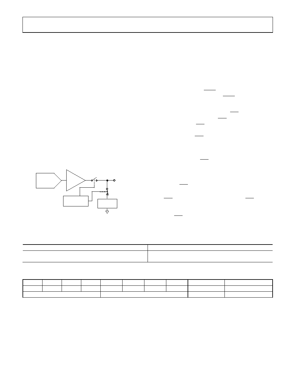
options. The output is connected internally to GND through
either a 1 k or a 100 k resistor, or it is left open-circuited
(three-state). The output stage is illustrated in Figure 55.
RESISTOR
NETWORK
VOUT
RESISTOR
STRING DAC
POWER-DOWN
CIRCUITRY
AMPLIFIER
08819-
051
Figure 55. Output Stage During Power-Down
The bias generator of the selected DAC(s), output amplifier,
resistor string, and other associated linear circuitry is shut down
when the power-down mode is activated. The internal reference
is powered down only when all channels are powered down.
However, the contents of the DAC register are unaffected when
in power-down. The time to exit power-down is typically 4 s
for VDD = 5 V and for VDD = 3 V.
Any combination of DACs can be powered up by setting PD1
and PD0 to 0 (normal operation). The output powers up to the
value in the input register (LDAC low) or to the value in the
DAC register before powering down (LDAC high).
CLEAR CODE REGISTER
The AD5629R/AD5669R have a hardware CLR pin that
is an asynchronous clear input. The CLR input is falling edge
sensitive. Bringing the CLR line low clears the contents of the
input register and the DAC registers to the data contained in
the user-configurable CLR register and sets the analog outputs
accordingly. This function can be used in system calibration to load
zero scale, midscale, or full scale to all channels together. These
clear code values are user-programmable by setting two bits, Bit
DB1 and Bit DB0, in the CLR control register (see Table 15).
The default setting clears the outputs to 0 V. Command 0101
is reserved for loading the clear code register (see Table 8).
The part exits clear code mode at the end of the next valid write
to the part. If CLR is activated during a write sequence, the write
is aborted.
The CLR pulse activation time (the falling edge of CLR to when
the output starts to change) is typically 280 ns. However, if
outside the DAC linear region, it typically takes 520 ns after
executing CLR for the output to start changing (see Figure 44).
See Table 14 for the contents of the input shift register during
the loading clear code register operation.
Table 10. Internal Reference Register
Internal REF Register (DB0)
Action
0
Reference off (default)
1
Reference on
Table 11. 32-Bit Input Shift Register Contents for Reference Set-Up Command
MSB
LSB
DB23
DB22
DB21
DB20
DB19
DB18
DB17
DB16
DB15 to DB1
DB0
1
0
X
1/0
Command bits (C3 to C0)
Address bits (A3 to A0)—don’t cares
Don’t cares
Internal REF on/off
相关PDF资料 |
PDF描述 |
|---|---|
| SY88149NDLMG TR | IC LIMITING AMP 1.25GBPS 16QFN |
| AD5629RBCPZ-1-RL7 | IC DAC 12BIT I2C/SRL 16LFCSP-WQ |
| AD5326ARU | IC DAC 12BIT QUAD W/BUFF 16TSSOP |
| LTC1654IGN#TRPBF | IC D/A CONV 14BIT R-R DUAL16SSOP |
| VE-2WD-IV-F4 | CONVERTER MOD DC/DC 85V 150W |
相关代理商/技术参数 |
参数描述 |
|---|---|
| AD5629RBRUZ-2 | 功能描述:IC DAC 12BIT I2C/SRL 16TSSOP RoHS:是 类别:集成电路 (IC) >> 数据采集 - 数模转换器 系列:denseDAC 标准包装:1 系列:- 设置时间:4.5µs 位数:12 数据接口:串行,SPI? 转换器数目:1 电压电源:单电源 功率耗散(最大):- 工作温度:-40°C ~ 125°C 安装类型:表面贴装 封装/外壳:8-SOIC(0.154",3.90mm 宽) 供应商设备封装:8-SOICN 包装:剪切带 (CT) 输出数目和类型:1 电压,单极;1 电压,双极 采样率(每秒):* 其它名称:MCP4921T-E/SNCTMCP4921T-E/SNRCTMCP4921T-E/SNRCT-ND |
| AD5629RBRUZ-2-RL7 | 功能描述:IC DAC 12BIT I2C/SRL 16TSSOP RoHS:是 类别:集成电路 (IC) >> 数据采集 - 数模转换器 系列:denseDAC 标准包装:47 系列:- 设置时间:2µs 位数:14 数据接口:并联 转换器数目:1 电压电源:单电源 功率耗散(最大):55µW 工作温度:-40°C ~ 85°C 安装类型:表面贴装 封装/外壳:28-SSOP(0.209",5.30mm 宽) 供应商设备封装:28-SSOP 包装:管件 输出数目和类型:1 电流,单极;1 电流,双极 采样率(每秒):* |
| AD562AD | 制造商:未知厂家 制造商全称:未知厂家 功能描述:12-Bit Digital-to-Analog Converter |
| AD562AD/BCD | 制造商:Rochester Electronics LLC 功能描述:- Bulk |
| AD562AD/BIN | 制造商:Rochester Electronics LLC 功能描述:- Bulk |
发布紧急采购,3分钟左右您将得到回复。