参数资料
| 型号: | AD565AJR |
| 厂商: | Analog Devices Inc |
| 文件页数: | 11/12页 |
| 文件大小: | 0K |
| 描述: | IC DAC 12BIT MONO 250NS 28-SOIC |
| 产品培训模块: | Data Converter Fundamentals DAC Architectures |
| 标准包装: | 1 |
| 设置时间: | 250ns |
| 位数: | 12 |
| 数据接口: | 并联 |
| 转换器数目: | 1 |
| 电压电源: | 单电源 |
| 功率耗散(最大): | 345mW |
| 工作温度: | 0°C ~ 70°C |
| 安装类型: | 表面贴装 |
| 封装/外壳: | 28-SOIC(0.295",7.50mm 宽) |
| 供应商设备封装: | 28-SOIC W |
| 包装: | 管件 |
| 输出数目和类型: | 1 电流,单极;1 电流,双极 |
| 采样率(每秒): | * |
AD565A/AD566A
REV.E
–8–
CONNECTING THE AD565A FOR BUFFERED VOLTAGE
OUTPUT
The standard current-to-voltage conversion connections using an
operational amplifier are shown in Figures 1, 2, and 3 with the
preferred trimming techniques. If a low offset operational amplifier
(OP77, AD741L, OP07) is used, excellent performance can be
obtained in many situations without trimming (an op amp with
less than 0.5 mV max offset voltage should be used to keep offset
errors below 1/2 LSB). If a 50
fixed resistor is substituted for
the 100
trimmer, unipolar zero is typically within ±1/2 LSB
(plus op amp offset) and full-scale accuracy is within 0.1%
(0.25% max). Substituting a 50
resistor for the 100 bipo-
lar offset trimmer gives a bipolar zero error typically within
±2 LSB (0.05%).
The AD509 is recommended for buffered voltage-output
applications that require a settling time to
± 1/2 LSB of
1
s. The feedback capacitor is shown with the optimum value
for each application; this capacitor is required to compen-
sate for the 25 pF DAC output capacitance.
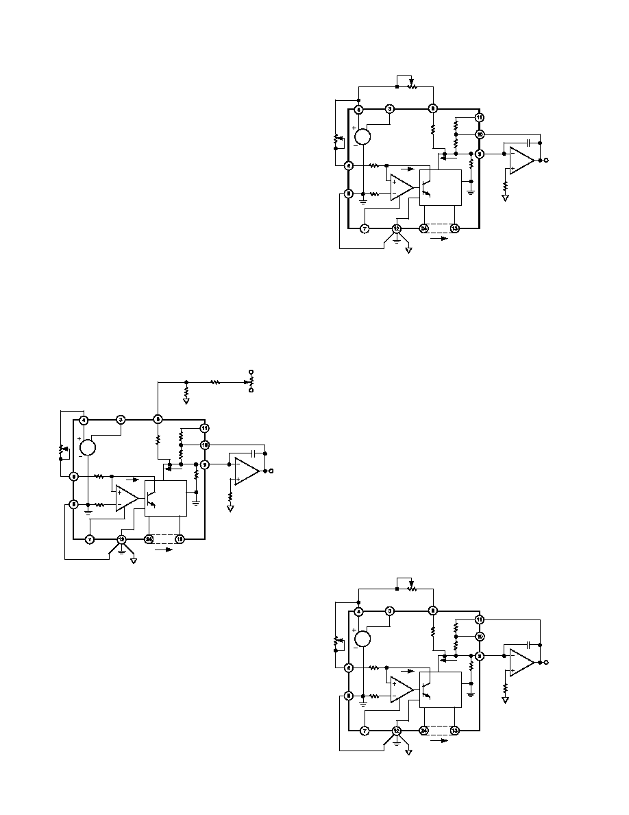
FIGURE 1. UNIPOLAR CONFIGURATION
This configuration provides a unipolar 0 V to 10 V output
range. In this mode, the bipolar terminal, Pin 8, should be
grounded if not used for trimming.
19.95k
20k
0.5mA
IREF
DAC
IOUT =
4
IREF
CODE
AD565A
9.95k
5k
8k
IO
20V SPAN
10V SPAN
DAC
OUT
POWER
GND
–VEE
REF
GND
BIPOLAR OFF
5k
CODE
INPUT
LSB
MSB
10V
VCC
REF
OUT
REF
IN
R2
100
10pF
AD509
OUTPUT
0V TO
+10V
100
100k
+15V
–15V
R1
50k
2.4k
Figure 1. 0 V to 10 V Unipolar Voltage Output
STEP I . . . ZERO ADJUST
Turn all bits OFF and adjust zero trimmer R1 until the output
reads 0.000 V (1 LSB = 2.44 mV). In most cases, this trim is not
needed, but Pin 8 should then be connected to Pin 12.
STEP II . . . GAIN ADJUST
Turn all bits ON and adjust 100
gain trimmer R2 until the
output is 9.9976 V. (Full scale is adjusted to 1 LSB less than
nominal full scale of 10.000 V.) If a 10.2375 V full scale is desired
(exactly 2.5 mV/bit), insert a 120
resistor in series with the gain
resistor at Pin 10 to the op amp output.
FIGURE 2. BIPOLAR CONFIGURATION
This configuration provides a bipolar output voltage from
–5.000 V to +4.9976 V, with positive full scale occurring with
all bits ON (all 1s).
19.95k
20k
0.5mA
IREF
DAC
IOUT =
4
IREF
CODE
AD565A
9.95k
5k
8k
IO
20V SPAN
10V SPAN
DAC
OUT
POWER
GND
–VEE
REF
GND
BIPOLAR OFF
5k
CODE
INPUT
LSB
MSB
10V
VCC
REF
OUT
REF
IN
R2
100
10pF
AD509
OUTPUT
–5V TO
+5V
2.4k
R1
100
Figure 2.
±5 V Bipolar Voltage Output
STEP I . . . OFFSET ADJUST
Turn OFF all bits. Adjust 100
trimmer R1 to give –5.000 V
output.
STEP II . . . GAIN ADJUST
Turn ON all bits. Adjust 100
gain trimmer R2 to give a
reading of +4.9976 V.
Please note that it is not necessary to trim the op amp to obtain
full accuracy at room temperature. In most bipolar situations,
an op amp trim is unnecessary unless the untrimmed offset drift
of the op amp is excessive.
FIGURE 3. OTHER VOLTAGE RANGES
The AD565A can also be easily configured for a unipolar 0 V to
+5 V range or
±2.5 V and ±10 V bipolar ranges by using the
additional 5 k
application resistor provided at the 20 V span R
terminal, Pin 11. For a 5 V span (0 V to +5 V, or
±2.5 V), the
two 5 k
resistors are used in parallel by shorting Pin 11 to Pin 9
and connecting Pin 10 to the op amp output and the bipolar
offset either to ground for unipolar or to REF OUT for the
bipolar offset either to ground for unipolar or to REF OUT for
the bipolar range. For the
±10 V range (20 V span) use the 5 k
resistors in series by connecting only Pin 11 to the op amp output
and the bipolar offset connected as shown. The
±10 V option is
shown in Figure 3.
19.95k
20k
0.5mA
IREF
DAC
IOUT =
4
IREF
CODE
AD565A
9.95k
5k
8k
IO
20V SPAN
10V SPAN
DAC
OUT
POWER
GND
–VEE
REF
GND
BIPOLAR OFF
5k
CODE
INPUT
LSB
MSB
10V
VCC
REF
OUT
REF
IN
R2
100
10pF
AD509
OUTPUT
–10V TO
+10V
3.0k
R1
100
Figure 3.
±10 V Voltage Output
相关PDF资料 |
PDF描述 |
|---|---|
| VE-B1T-MX-S | CONVERTER MOD DC/DC 6.5V 75W |
| AD9787BSVZRL | IC DAC 14BIT 800MSPS 100TQFP |
| VI-B1T-MX-S | CONVERTER MOD DC/DC 6.5V 75W |
| VE-B1W-MX-S | CONVERTER MOD DC/DC 5.5V 75W |
| AD7549JNZ | IC DAC 12BIT LC2MOS DUAL 20DIP |
相关代理商/技术参数 |
参数描述 |
|---|---|
| AD565AJR-REEL | 制造商:Analog Devices 功能描述:IC, MONO 12-BIT D/A CONV - Tape and Reel 制造商:Rochester Electronics LLC 功能描述:IC, MONO 12-BIT D/A CONV - Tape and Reel |
| AD565AJRZ | 功能描述:IC DAC 12BIT MONO 250NS 28SOIC RoHS:是 类别:集成电路 (IC) >> 数据采集 - 数模转换器 系列:- 产品培训模块:Data Converter Fundamentals DAC Architectures 标准包装:750 系列:- 设置时间:7µs 位数:16 数据接口:并联 转换器数目:1 电压电源:双 ± 功率耗散(最大):100mW 工作温度:0°C ~ 70°C 安装类型:表面贴装 封装/外壳:28-LCC(J 形引线) 供应商设备封装:28-PLCC(11.51x11.51) 包装:带卷 (TR) 输出数目和类型:1 电压,单极;1 电压,双极 采样率(每秒):143k |
| AD565AJRZ-REEL | 功能描述:IC DAC 12BIT MONO 250NS 28SOIC RoHS:是 类别:集成电路 (IC) >> 数据采集 - 数模转换器 系列:- 产品培训模块:Data Converter Fundamentals DAC Architectures 标准包装:750 系列:- 设置时间:7µs 位数:16 数据接口:并联 转换器数目:1 电压电源:双 ± 功率耗散(最大):100mW 工作温度:0°C ~ 70°C 安装类型:表面贴装 封装/外壳:28-LCC(J 形引线) 供应商设备封装:28-PLCC(11.51x11.51) 包装:带卷 (TR) 输出数目和类型:1 电压,单极;1 电压,双极 采样率(每秒):143k |
| AD565AK | 制造商:AD 制造商全称:Analog Devices 功能描述:High Speed 12-Bit Monolithic D/A Converters |
| AD565AKCWG | 制造商:未知厂家 制造商全称:未知厂家 功能描述:12-Bit Digital-to-Analog Converter |
发布紧急采购,3分钟左右您将得到回复。