- 您现在的位置:买卖IC网 > PDF目录9004 > AD5662BRJZ-1REEL7 (Analog Devices Inc)IC DAC 16BIT BUFF V-OUT SOT23-8 PDF资料下载
参数资料
| 型号: | AD5662BRJZ-1REEL7 |
| 厂商: | Analog Devices Inc |
| 文件页数: | 11/24页 |
| 文件大小: | 0K |
| 描述: | IC DAC 16BIT BUFF V-OUT SOT23-8 |
| 产品培训模块: | Data Converter Fundamentals DAC Architectures |
| 设计资源: | 4 mA to 20 mA Process Control Loop Using AD5662 (CN0009) 16-Bit Fully Isolated Voltage Output Module Using AD5662, ADuM1401, and External Amplifiers (CN0063) 16-Bit Fully Isolated 4 mA to 20 mA Output Module Using AD5662, ADuM1401, and External Amplifiers (CN0064) |
| 标准包装: | 1 |
| 系列: | nanoDAC™ |
| 设置时间: | 8µs |
| 位数: | 16 |
| 数据接口: | DSP,MICROWIRE?,QSPI?,串行,SPI? |
| 转换器数目: | 1 |
| 电压电源: | 单电源 |
| 工作温度: | -40°C ~ 125°C |
| 安装类型: | 表面贴装 |
| 封装/外壳: | SOT-23-8 |
| 供应商设备封装: | SOT-23-8 |
| 包装: | 标准包装 |
| 输出数目和类型: | 1 电压,单极 |
| 产品目录页面: | 783 (CN2011-ZH PDF) |
| 其它名称: | AD5662BRJZ-1REEL7DKR |
AD5662
Rev. A | Page 19 of 24
BIPOLAR OPERATION USING THE AD5662
The AD5662 has been designed for single-supply operation,
but a bipolar output range is also possible using the circuit in
Figure 42. The circuit gives an output voltage range of ±5 V.
Rail-to-rail operation at the amplifier output is achievable using
an AD820 or an OP295 as the output amplifier.
The output voltage for any input code can be calculated as
follows:
×
+
×
×
=
R1
R2
V
R1
R2
R1
D
V
DD
O
536
,
65
where D represents the input code in decimal (0 to 65,535).
With VDD = 5 V, R1 = R2 = 10 kΩ,
V
5
536
,
65
10
×
=
D
VO
This is an output voltage range of ±5 V, with 0x0000 corre-
sponding to a 5 V output, and 0xFFFF corresponding to a
+5 V output.
R2 = 10k
Ω
04777-032
+5V
–5V
AD820/
OP295
THREE-WIRE
SERIAL
INTERFACE
+5V
AD5662
VREF
VOUT
VFB
R1 = 10k
Ω
±5V
0.1
μF
10
μF
Figure 42. Bipolar Operation with the AD5662
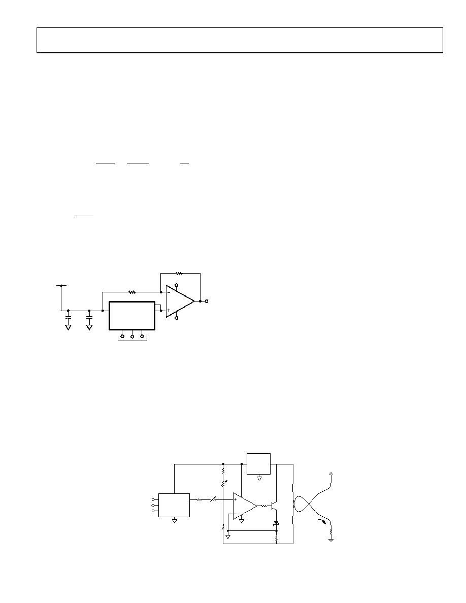
USING THE AD5662 AS AN ISOLATED,
PROGRAMMABLE, 4-20 mA PROCESS
CONTROLLER
In many process control system applications, 2-wire current
transmitters are used to transmit analog signals through noisy
environments. These current transmitters use a zero-scale
signal current of 4 mA that can power the transmitter’s signal
conditioning circuitry. The full-scale output signal in these
transmitters is 20 mA. The converse approach to process
control can also be used; a low-power, programmable current
source can be used to control remotely located sensors or
devices in the loop.
A circuit that performs this function is shown in Figure 43.
Using the AD5662 as the controller, the circuit provides a
programmable output current of 4 mA to 20 mA, proportional
to the DAC’s digital code. Biasing for the controller is provided
by the ADR02 and requires no external trim for two reasons:
(1) the ADR02’s tight initial output voltage tolerance and (2)
the low supply current consumption of both the AD8627 and
the AD5662. The entire circuit, including opto-couplers,
consumes less than 3 mA from the total budget of 4 mA. The
AD8627 regulates the output current to satisfy the current
summation at the noninverting node of the AD8627.
IOUT = 1/R7 (VDAC × R3/R1 + VREF × R3/R2)
For the values shown in Figure 43,
IOUT = 0.2435 μA × D + 4 mA
where D = 0 ≤ D ≤ 65535, giving a full-scale output current of
20 mA when the AD5662’s digital code equals 0xFFFF. Offset
trim at 4 mA is provided by P2, and P1 provides the circuit’s
gain trim at 20 mA. These two trims do not interact because
the noninverting input of the AD8627 is at virtual ground. The
Schottky diode, D1, is required in this circuit to prevent loop
supply power-on transients from pulling the noninverting input
of the AD8627 more than 300 mV below its inverting input.
Without this diode, such transients could cause phase reversal
of the AD8627 and possible latch-up of the controller. The loop
supply voltage compliance of the circuit is limited by the maxi-
mum applied input voltage to the ADR02 and is from 12 V to
40 V.
04777-
034
SERIAL
LOAD
AD5662
VLOOP
12V TO 36V
4mA TO 20mA
AD8627
R1
4.7k
Ω
R2
18.5k
Ω
P1
20mA
ADJUST
P2
4mA
ADJUST
R6
3.3k
Ω
R3
1.5k
Ω
D1
Q1
2N3904
R7
100
Ω
RL
ADR02
Figure 43. Programmable 4–20 mA Process Controller
相关PDF资料 |
PDF描述 |
|---|---|
| MPC9239AC | IC CLK SYNTH LV PECL 32-LQFP |
| VE-BN1-MV-F3 | CONVERTER MOD DC/DC 12V 150W |
| MK2772-01SLF | IC CLK SRC VCXO/SET-TOP 20-SOIC |
| VE-BN1-MV-F1 | CONVERTER MOD DC/DC 12V 150W |
| VE-BN0-MV-F3 | CONVERTER MOD DC/DC 5V 150W |
相关代理商/技术参数 |
参数描述 |
|---|---|
| AD5662BRJZ-2500RL7 | 功能描述:IC DAC 16BIT BUFF V-OUT SOT23-8 RoHS:是 类别:集成电路 (IC) >> 数据采集 - 数模转换器 系列:nanoDAC™ 产品培训模块:Lead (SnPb) Finish for COTS Obsolescence Mitigation Program 标准包装:50 系列:- 设置时间:4µs 位数:12 数据接口:串行 转换器数目:2 电压电源:单电源 功率耗散(最大):- 工作温度:-40°C ~ 85°C 安装类型:表面贴装 封装/外壳:8-TSSOP,8-MSOP(0.118",3.00mm 宽) 供应商设备封装:8-uMAX 包装:管件 输出数目和类型:2 电压,单极 采样率(每秒):* 产品目录页面:1398 (CN2011-ZH PDF) |
| AD5662BRJZ-2REEL7 | 功能描述:IC DAC 16BIT BUFF V-OUT SOT23-8 RoHS:是 类别:集成电路 (IC) >> 数据采集 - 数模转换器 系列:nanoDAC™ 产品培训模块:Data Converter Fundamentals DAC Architectures 标准包装:3,000 系列:nanoDAC™ 设置时间:80µs 位数:18 数据接口:DSP,MICROWIRE?,QSPI?,串行,SPI? 转换器数目:1 电压电源:单电源 功率耗散(最大):- 工作温度:-40°C ~ 105°C 安装类型:表面贴装 封装/外壳:SOT-23-8 供应商设备封装:SOT-23-8 包装:带卷 (TR) 输出数目和类型:1 电压,单极 采样率(每秒):- 产品目录页面:784 (CN2011-ZH PDF) 配用:EVAL-AD5680EBZ-ND - BOARD EVAL FOR AD5680 其它名称:AD5680BRJZ-2REEL7TR |
| AD5662BRM | 制造商:AD 制造商全称:Analog Devices 功能描述:2.7 V to 5.5 V, 250 ??A, Rail-to-Rail Output 16-Bit DAC D/A in a SOT-23 |
| AD5662BRM-1 | 功能描述:IC DAC 16BIT BUFF V-OUT 8-MSOP RoHS:否 类别:集成电路 (IC) >> 数据采集 - 数模转换器 系列:nanoDAC™ 标准包装:47 系列:- 设置时间:2µs 位数:14 数据接口:并联 转换器数目:1 电压电源:单电源 功率耗散(最大):55µW 工作温度:-40°C ~ 85°C 安装类型:表面贴装 封装/外壳:28-SSOP(0.209",5.30mm 宽) 供应商设备封装:28-SSOP 包装:管件 输出数目和类型:1 电流,单极;1 电流,双极 采样率(每秒):* |
| AD5662BRM-1REEL7 | 功能描述:IC DAC 16BIT BUFF V-OUT 8-MSOP RoHS:否 类别:集成电路 (IC) >> 数据采集 - 数模转换器 系列:nanoDAC™ 产品培训模块:LTC263x 12-, 10-, and 8-Bit VOUT DAC Family 特色产品:LTC2636 - Octal 12-/10-/8-Bit SPI VOUT DACs with 10ppm/°C Reference 标准包装:91 系列:- 设置时间:4µs 位数:10 数据接口:MICROWIRE?,串行,SPI? 转换器数目:8 电压电源:单电源 功率耗散(最大):2.7mW 工作温度:-40°C ~ 85°C 安装类型:表面贴装 封装/外壳:14-WFDFN 裸露焊盘 供应商设备封装:14-DFN-EP(4x3) 包装:管件 输出数目和类型:8 电压,单极 采样率(每秒):* |
发布紧急采购,3分钟左右您将得到回复。