- 您现在的位置:买卖IC网 > PDF目录9004 > AD5662BRJZ-1REEL7 (Analog Devices Inc)IC DAC 16BIT BUFF V-OUT SOT23-8 PDF资料下载
参数资料
| 型号: | AD5662BRJZ-1REEL7 |
| 厂商: | Analog Devices Inc |
| 文件页数: | 7/24页 |
| 文件大小: | 0K |
| 描述: | IC DAC 16BIT BUFF V-OUT SOT23-8 |
| 产品培训模块: | Data Converter Fundamentals DAC Architectures |
| 设计资源: | 4 mA to 20 mA Process Control Loop Using AD5662 (CN0009) 16-Bit Fully Isolated Voltage Output Module Using AD5662, ADuM1401, and External Amplifiers (CN0063) 16-Bit Fully Isolated 4 mA to 20 mA Output Module Using AD5662, ADuM1401, and External Amplifiers (CN0064) |
| 标准包装: | 1 |
| 系列: | nanoDAC™ |
| 设置时间: | 8µs |
| 位数: | 16 |
| 数据接口: | DSP,MICROWIRE?,QSPI?,串行,SPI? |
| 转换器数目: | 1 |
| 电压电源: | 单电源 |
| 工作温度: | -40°C ~ 125°C |
| 安装类型: | 表面贴装 |
| 封装/外壳: | SOT-23-8 |
| 供应商设备封装: | SOT-23-8 |
| 包装: | 标准包装 |
| 输出数目和类型: | 1 电压,单极 |
| 产品目录页面: | 783 (CN2011-ZH PDF) |
| 其它名称: | AD5662BRJZ-1REEL7DKR |
AD5662
Rev. A | Page 15 of 24
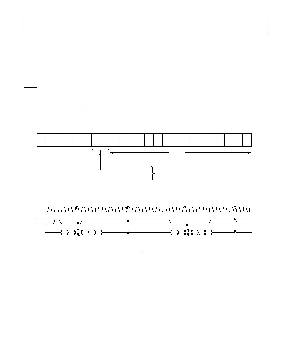
INPUT SHIFT REGISTER
The input shift register is 24 bits wide (see Figure 34). The first
six bits are don’t cares. The next two are control bits that control
the part’s mode of operation (normal mode or any one of three
power-down modes). See the Power-Down Modes section for a
more complete description of the various modes. The next 16
bits are the data bits. These are transferred to the DAC register
on the 24th falling edge of SCLK.
SYNC INTERRUPT
In a normal write sequence, the SYNC line is kept low for at
least 24 falling edges of SCLK, and the DAC is updated on the
24th falling edge. However, if SYNC is brought high before the
24th falling edge, this acts as an interrupt to the write sequence.
The shift register is reset and the write sequence is seen as
invalid. Neither an update of the DAC register contents nor a
change in the operating mode occurs (see
).
POWER-ON RESET
The AD5662 family contains a power-on reset circuit that
controls the output voltage during power-up. The AD5662x-1
DAC output powers up to 0 V, and the AD5662x-2 DAC output
powers up to midscale. The output remains there until a valid
write sequence is made to the DAC. This is useful in
applications where it is important to know the state of the
output of the DAC while it is in the process of powering up.
DATA BITS
DB23 (MSB)
PD1
PD0
D15
D14
D13
D12
X
D11
D10
D9
D8
D7
D6
D5
D4
D3
D2
DBO (LSB)
D1
D0
NORMAL OPERATION
1 k
Ω TO GND
100 k
Ω TO GND
THREE-STATE
POWER-DOWN MODES
0
1
0
1
0
1
04777-024
Figure 34. Input Register Contents
04777-025
DIN
DB23
DB0
INVALID WRITE SEQUENCE:
SYNC HIGH BEFORE 24TH FALLING EDGE
VALID WRITE SEQUENCE, OUTPUT UPDATES
ON THE 24TH FALLING EDGE
SYNC
SCLK
Figure 35. SYNC Interrupt Facility
相关PDF资料 |
PDF描述 |
|---|---|
| MPC9239AC | IC CLK SYNTH LV PECL 32-LQFP |
| VE-BN1-MV-F3 | CONVERTER MOD DC/DC 12V 150W |
| MK2772-01SLF | IC CLK SRC VCXO/SET-TOP 20-SOIC |
| VE-BN1-MV-F1 | CONVERTER MOD DC/DC 12V 150W |
| VE-BN0-MV-F3 | CONVERTER MOD DC/DC 5V 150W |
相关代理商/技术参数 |
参数描述 |
|---|---|
| AD5662BRJZ-2500RL7 | 功能描述:IC DAC 16BIT BUFF V-OUT SOT23-8 RoHS:是 类别:集成电路 (IC) >> 数据采集 - 数模转换器 系列:nanoDAC™ 产品培训模块:Lead (SnPb) Finish for COTS Obsolescence Mitigation Program 标准包装:50 系列:- 设置时间:4µs 位数:12 数据接口:串行 转换器数目:2 电压电源:单电源 功率耗散(最大):- 工作温度:-40°C ~ 85°C 安装类型:表面贴装 封装/外壳:8-TSSOP,8-MSOP(0.118",3.00mm 宽) 供应商设备封装:8-uMAX 包装:管件 输出数目和类型:2 电压,单极 采样率(每秒):* 产品目录页面:1398 (CN2011-ZH PDF) |
| AD5662BRJZ-2REEL7 | 功能描述:IC DAC 16BIT BUFF V-OUT SOT23-8 RoHS:是 类别:集成电路 (IC) >> 数据采集 - 数模转换器 系列:nanoDAC™ 产品培训模块:Data Converter Fundamentals DAC Architectures 标准包装:3,000 系列:nanoDAC™ 设置时间:80µs 位数:18 数据接口:DSP,MICROWIRE?,QSPI?,串行,SPI? 转换器数目:1 电压电源:单电源 功率耗散(最大):- 工作温度:-40°C ~ 105°C 安装类型:表面贴装 封装/外壳:SOT-23-8 供应商设备封装:SOT-23-8 包装:带卷 (TR) 输出数目和类型:1 电压,单极 采样率(每秒):- 产品目录页面:784 (CN2011-ZH PDF) 配用:EVAL-AD5680EBZ-ND - BOARD EVAL FOR AD5680 其它名称:AD5680BRJZ-2REEL7TR |
| AD5662BRM | 制造商:AD 制造商全称:Analog Devices 功能描述:2.7 V to 5.5 V, 250 ??A, Rail-to-Rail Output 16-Bit DAC D/A in a SOT-23 |
| AD5662BRM-1 | 功能描述:IC DAC 16BIT BUFF V-OUT 8-MSOP RoHS:否 类别:集成电路 (IC) >> 数据采集 - 数模转换器 系列:nanoDAC™ 标准包装:47 系列:- 设置时间:2µs 位数:14 数据接口:并联 转换器数目:1 电压电源:单电源 功率耗散(最大):55µW 工作温度:-40°C ~ 85°C 安装类型:表面贴装 封装/外壳:28-SSOP(0.209",5.30mm 宽) 供应商设备封装:28-SSOP 包装:管件 输出数目和类型:1 电流,单极;1 电流,双极 采样率(每秒):* |
| AD5662BRM-1REEL7 | 功能描述:IC DAC 16BIT BUFF V-OUT 8-MSOP RoHS:否 类别:集成电路 (IC) >> 数据采集 - 数模转换器 系列:nanoDAC™ 产品培训模块:LTC263x 12-, 10-, and 8-Bit VOUT DAC Family 特色产品:LTC2636 - Octal 12-/10-/8-Bit SPI VOUT DACs with 10ppm/°C Reference 标准包装:91 系列:- 设置时间:4µs 位数:10 数据接口:MICROWIRE?,串行,SPI? 转换器数目:8 电压电源:单电源 功率耗散(最大):2.7mW 工作温度:-40°C ~ 85°C 安装类型:表面贴装 封装/外壳:14-WFDFN 裸露焊盘 供应商设备封装:14-DFN-EP(4x3) 包装:管件 输出数目和类型:8 电压,单极 采样率(每秒):* |
发布紧急采购,3分钟左右您将得到回复。