参数资料
| 型号: | AD5663BRMZ-1 |
| 厂商: | Analog Devices Inc |
| 文件页数: | 10/24页 |
| 文件大小: | 0K |
| 描述: | IC DAC NANO 16BIT DUAL 10-MSOP |
| 产品培训模块: | Data Converter Fundamentals DAC Architectures |
| 标准包装: | 50 |
| 系列: | nanoDAC™ |
| 设置时间: | 4µs |
| 位数: | 16 |
| 数据接口: | 串行 |
| 转换器数目: | 2 |
| 电压电源: | 单电源 |
| 功率耗散(最大): | 2.5mW |
| 工作温度: | -40°C ~ 105°C |
| 安装类型: | 表面贴装 |
| 封装/外壳: | 10-TFSOP,10-MSOP(0.118",3.00mm 宽) |
| 供应商设备封装: | 10-MSOP |
| 包装: | 管件 |
| 输出数目和类型: | 2 电压,单极;2 电压,双极 |
| 采样率(每秒): | 220k |
| 产品目录页面: | 783 (CN2011-ZH PDF) |
| 配用: | EVAL-AD5663REBZ-ND - BOARD EVAL FOR AD5663 |
AD5663
Rev. 0 | Page 18 of 24
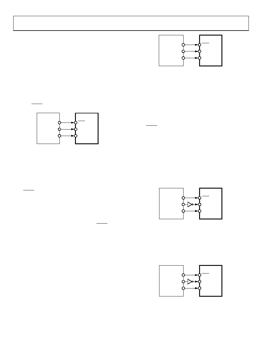
MICROPROCESSOR INTERFACING
AD5663 to Blackfin ADSP BF53x Interface
Figure 32 shows a serial interface between the AD5663 and the
Blackfin ADSP-BF53x microprocessor. The ADSP-BF53x processor
family incorporates two dual-channel synchronous serial ports,
SPORT1 and SPORT0, for serial and multiprocessor
communications. Using SPORT0 to connect to the AD5663, the
setup for the interface is as follows:
DT0PRI drives the DIN pin of the AD5663.
TSCLK0 drives the SCLK of the part.
The SYNC pin is driven from TFS0.
AD56631
ADSP-BF53x1
SYNC
TFS0
DIN
DTOPRI
SCLK
TSCLK0
1ADDITIONAL PINS OMITTED FOR CLARITY.
05
85
5-
0
3
7
Figure 32. AD5663 to Blackfin ADSP-BF53x Interface
AD5663 to 68HC11/68L11 Interface
Figure 33 shows a serial interface between the AD5663 and the
68HC11/68L11 microcontroller. SCK of the 68HC11/68L11
drives the SCLK of the AD5663, and the MOSI output drives
the serial data line of the DAC.
The SYNC signal is derived from a port line (PC7). The setup
conditions for correct operation of this interface are as follows:
The 68HC11/68L11 is configured with its CPOL bit as 0.
The 68HC11/68L11 is configured with its CPHA bit as 1.
When data is being transmitted to the DAC, the SYNC line is
taken low (PC7). When the 68HC11/68L11 is configured as
previously described, data appearing on the MOSI output is
valid on the falling edge of SCK. Serial data from the
68HC11/68L11 is transmitted in 10-bit bytes with only eight
falling clock edges occurring in the transmit cycle. Data is
transmitted MSB first. To load data to the AD5663, PC7 is left
low after the first eight bits are transferred, and a second serial
write operation is performed to the DAC. PC7 is taken high at
the end of this procedure.
AD56631
68HC11/68L111
SYNC
PC7
SCLK
SCK
DIN
MOSI
1ADDITIONAL PINS OMITTED FOR CLARITY.
05
85
5-
0
3
8
Figure 33. AD5663 to 68HC11/68L11 Interface
AD5663 to 80C51/80L51 Interface
Figure 34 shows a serial interface between the AD5663 and the
80C51/80L51 microcontroller. The setup for the interface is as
follows:
TxD of the 80C51/80L51 drives SCLK of the AD5663.
RxD drives the serial data line of the part.
The SYNC signal is again derived from a bit-programmable pin
on the port. In this case, Port Line P3.3 is used. When data is to be
transmitted to the AD5663, P3.3 is taken low. The 80C51/80L51
transmits data in 10-bit bytes only; thus only eight falling clock
edges occur in the transmit cycle. To load data to the DAC, P3.3
is left low after the first eight bits are transmitted, and a second
write cycle is initiated to transmit the second byte of data. P3.3
is taken high following the completion of this cycle. The 80C51/
80L51 outputs the serial data in a format that has the LSB first.
The AD5663 must receive data with the MSB first. The 80C51/
80L51 transmit routine should take this into account.
AD56631
80C51/80L511
SYNC
P3.3
SCLK
TxD
DIN
RxD
1ADDITIONAL PINS OMITTED FOR CLARITY.
05
85
5-
0
3
9
Figure 34. AD5663 to 80C51/80L51 Interface
AD5663 to MICROWIRE Interface
Figure 35 shows an interface between the AD5663 and any
MICROWIRE-compatible device. Serial data is shifted out on
the falling edge of the serial clock and is clocked into the AD5663
on the rising edge of the SK.
AD56631
MICROWIRE1
SYNC
CS
SCLK
SK
DIN
SO
1ADDITIONAL PINS OMITTED FOR CLARITY.
05
85
5-
0
4
0
Figure 35. AD5663 to MICROWIRE Interface
相关PDF资料 |
PDF描述 |
|---|---|
| VI-2TV-MY-F2 | CONVERTER MOD DC/DC 5.8V 50W |
| VI-2TT-MY-F4 | CONVERTER MOD DC/DC 6.5V 50W |
| VE-J53-MZ-F1 | CONVERTER MOD DC/DC 24V 25W |
| VI-2TT-MY-F3 | CONVERTER MOD DC/DC 6.5V 50W |
| CS4385-DQZ | IC DAC 8CH 114DB 192KHZ 48LQFP |
相关代理商/技术参数 |
参数描述 |
|---|---|
| AD5663BRMZ-1REEL7 | 功能描述:IC DAC 16BIT DUAL 10-MSOP RoHS:是 类别:集成电路 (IC) >> 数据采集 - 数模转换器 系列:nanoDAC™ 产品培训模块:LTC263x 12-, 10-, and 8-Bit VOUT DAC Family 特色产品:LTC2636 - Octal 12-/10-/8-Bit SPI VOUT DACs with 10ppm/°C Reference 标准包装:91 系列:- 设置时间:4µs 位数:10 数据接口:MICROWIRE?,串行,SPI? 转换器数目:8 电压电源:单电源 功率耗散(最大):2.7mW 工作温度:-40°C ~ 85°C 安装类型:表面贴装 封装/外壳:14-WFDFN 裸露焊盘 供应商设备封装:14-DFN-EP(4x3) 包装:管件 输出数目和类型:8 电压,单极 采样率(每秒):* |
| AD5663BRMZ-REEL7 | 功能描述:IC DAC 16BIT DUAL 10-MSOP RoHS:是 类别:集成电路 (IC) >> 数据采集 - 数模转换器 系列:nanoDAC™ 产品培训模块:LTC263x 12-, 10-, and 8-Bit VOUT DAC Family 特色产品:LTC2636 - Octal 12-/10-/8-Bit SPI VOUT DACs with 10ppm/°C Reference 标准包装:91 系列:- 设置时间:4µs 位数:10 数据接口:MICROWIRE?,串行,SPI? 转换器数目:8 电压电源:单电源 功率耗散(最大):2.7mW 工作温度:-40°C ~ 85°C 安装类型:表面贴装 封装/外壳:14-WFDFN 裸露焊盘 供应商设备封装:14-DFN-EP(4x3) 包装:管件 输出数目和类型:8 电压,单极 采样率(每秒):* |
| AD5663R | 制造商:AD 制造商全称:Analog Devices 功能描述:Dual 12-/14-/16-Bit nanoDAC with 5 ppm/C On-Chip Reference |
| AD5663RBCPZ-3R2 | 功能描述:IC DAC NANO 16BIT DUAL 10-LFCSP RoHS:是 类别:集成电路 (IC) >> 数据采集 - 数模转换器 系列:nanoDAC™ 标准包装:47 系列:- 设置时间:2µs 位数:14 数据接口:并联 转换器数目:1 电压电源:单电源 功率耗散(最大):55µW 工作温度:-40°C ~ 85°C 安装类型:表面贴装 封装/外壳:28-SSOP(0.209",5.30mm 宽) 供应商设备封装:28-SSOP 包装:管件 输出数目和类型:1 电流,单极;1 电流,双极 采样率(每秒):* |
| AD5663RBCPZ-3REEL7 | 功能描述:IC DAC NANO 16BIT 1.25V 10-LFCSP RoHS:是 类别:集成电路 (IC) >> 数据采集 - 数模转换器 系列:nanoDAC™ 产品培训模块:LTC263x 12-, 10-, and 8-Bit VOUT DAC Family 特色产品:LTC2636 - Octal 12-/10-/8-Bit SPI VOUT DACs with 10ppm/°C Reference 标准包装:91 系列:- 设置时间:4µs 位数:10 数据接口:MICROWIRE?,串行,SPI? 转换器数目:8 电压电源:单电源 功率耗散(最大):2.7mW 工作温度:-40°C ~ 85°C 安装类型:表面贴装 封装/外壳:14-WFDFN 裸露焊盘 供应商设备封装:14-DFN-EP(4x3) 包装:管件 输出数目和类型:8 电压,单极 采样率(每秒):* |
发布紧急采购,3分钟左右您将得到回复。