参数资料
| 型号: | AD5663BRMZ-1 |
| 厂商: | Analog Devices Inc |
| 文件页数: | 8/24页 |
| 文件大小: | 0K |
| 描述: | IC DAC NANO 16BIT DUAL 10-MSOP |
| 产品培训模块: | Data Converter Fundamentals DAC Architectures |
| 标准包装: | 50 |
| 系列: | nanoDAC™ |
| 设置时间: | 4µs |
| 位数: | 16 |
| 数据接口: | 串行 |
| 转换器数目: | 2 |
| 电压电源: | 单电源 |
| 功率耗散(最大): | 2.5mW |
| 工作温度: | -40°C ~ 105°C |
| 安装类型: | 表面贴装 |
| 封装/外壳: | 10-TFSOP,10-MSOP(0.118",3.00mm 宽) |
| 供应商设备封装: | 10-MSOP |
| 包装: | 管件 |
| 输出数目和类型: | 2 电压,单极;2 电压,双极 |
| 采样率(每秒): | 220k |
| 产品目录页面: | 783 (CN2011-ZH PDF) |
| 配用: | EVAL-AD5663REBZ-ND - BOARD EVAL FOR AD5663 |
AD5663
Rev. 0 | Page 16 of 24
POWER-DOWN MODES
The AD5663 contains four separate modes of operation.
Command 100 is reserved for the power-down function
(see Table 7). These modes are software-programmable by
setting Bit DB5 and Bit DB4 in the control register. Table 11
shows how the state of the bits corresponds to the mode of
operation of the device. Any or all DACs (DAC B and DAC A)
can be powered down to the selected mode by setting the
corresponding two bits (Bit DB1 and Bit DB0) to 1. By
executing the same Command 100, any combination of DACs
can be powered up by setting Bit DB5 and Bit DB4 to normal
operation mode. Again, to select which combination of DAC
channels to power up, set the corresponding two bits (Bit DB1
and Bit DB0) to 1. See Table 12 for contents of the input shift
register during power-down/power-up operation.
The DAC output powers up to the value in the input register
while LDAC is low. If LDAC is high, the DAC output powers up
to the value held in the DAC register before power-down.
When both bits are set to 0, the part works normally with its
normal power consumption of 500 μA at 5 V. However, for the
three power-down modes, the supply current falls to 480 nA at
5 V (100 nA at 3 V). Not only does the supply current fall, but
the output stage is also internally switched from the output of
the amplifier to a resistor network of known values. This has the
advantage that the output impedance of the part is known while
the part is in power-down mode. The outputs can either be
connected internally to GND through a 1 kΩ or 100 kΩ register
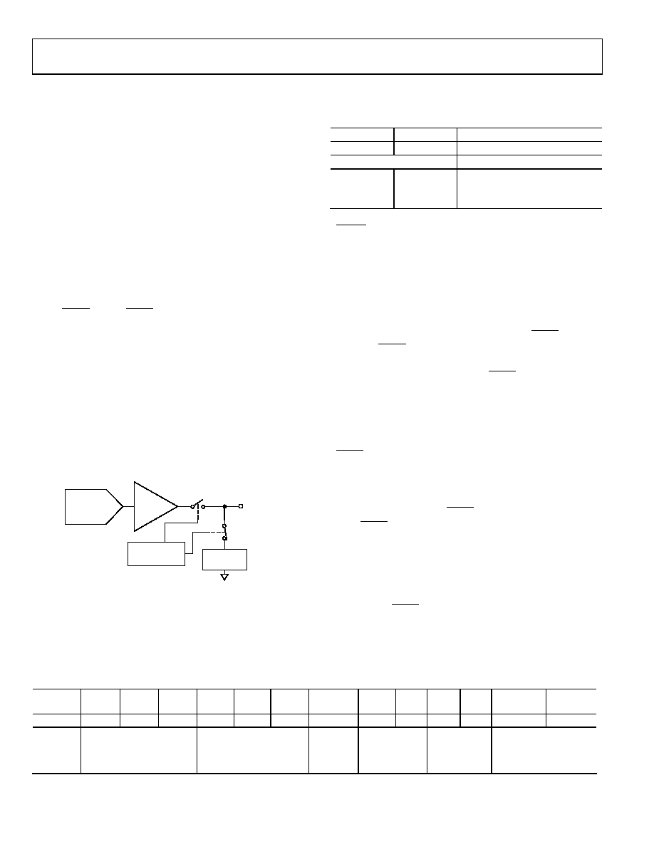
or left open-circuited (three-state) (see Figure 31).
RESISTOR
NETWORK
VOUT
RESISTOR
STRING DAC
POWER-DOWN
CIRCUITRY
AMPLIFIER
05
85
5-
0
36
Figure 31. Output Stage During Power-Down
The bias generator, the output amplifier, the resistor string, and
other associated linear circuitry are shut down when power-
down mode is activated. However, the contents of the DAC
register are unaffected when in power-down.
The time required to exit power-down is typically 4 μs for
Table 11. Power-Down Modes of Operation for the AD5663
DB5
DB4
Operating Mode
0
Normal operation
Power-Down Modes
0
1
1 kΩ to GND
1
0
100 kΩ to GND
1
Three-state
LDAC FUNCTION
The AD5663 DAC has double-buffered interfaces consisting of
two banks of registers: input registers and DAC registers. The
input registers are connected directly to the input shift register
and the digital code is transferred to the relevant input register
on completion of a valid write sequence. The DAC registers
contain the digital code used by the resistor strings.
Access to the DAC registers is controlled by the LDAC pin.
When the LDAC pin is high, the DAC registers are latched and
the input registers can change state without affecting the
contents of the DAC registers. When LDAC is brought low,
however, the DAC registers become transparent and the
contents of the input registers are transferred to them. The
double-buffered interface is useful if the user requires
simultaneous updating of all DAC outputs. The user can write
to one of the input registers individually and then, by bringing
LDAC low when writing to the other DAC input register, all
outputs update simultaneously.
These parts each contain an extra feature whereby a DAC
register is not updated unless its input register has been
updated since the last time LDAC was brought low. Normally,
when LDAC is brought low, the DAC registers are filled with
the contents of the input registers. In the case of the AD5663,
the DAC register updates only if the input register has changed
since the last time the DAC register was updated, thereby
removing unnecessary digital crosstalk.
The outputs of all DACs can be updated simultaneously using
the hardware LDAC pin.
Table 12. 24-Bit Input Shift Register Contents of Power-Up/Power-Down Function
MSB
LSB
DB23 to
DB22
DB21
DB20
DB19
DB18
DB17
DB16
DB15 to
DB6
DB5
DB4
DB3
DB2
DB1
DB0
x
1
0
x
PD1
PD0
x
DAC B
DAC A
Don’t
care
Command bits (C2 to C0)
Address bits (A2 to A0);
don’t care
Don’t
care
Power-down
mode
Don’t care
Power down/Power up
channel selection;
set bit to 1 to select
channel
相关PDF资料 |
PDF描述 |
|---|---|
| VI-2TV-MY-F2 | CONVERTER MOD DC/DC 5.8V 50W |
| VI-2TT-MY-F4 | CONVERTER MOD DC/DC 6.5V 50W |
| VE-J53-MZ-F1 | CONVERTER MOD DC/DC 24V 25W |
| VI-2TT-MY-F3 | CONVERTER MOD DC/DC 6.5V 50W |
| CS4385-DQZ | IC DAC 8CH 114DB 192KHZ 48LQFP |
相关代理商/技术参数 |
参数描述 |
|---|---|
| AD5663BRMZ-1REEL7 | 功能描述:IC DAC 16BIT DUAL 10-MSOP RoHS:是 类别:集成电路 (IC) >> 数据采集 - 数模转换器 系列:nanoDAC™ 产品培训模块:LTC263x 12-, 10-, and 8-Bit VOUT DAC Family 特色产品:LTC2636 - Octal 12-/10-/8-Bit SPI VOUT DACs with 10ppm/°C Reference 标准包装:91 系列:- 设置时间:4µs 位数:10 数据接口:MICROWIRE?,串行,SPI? 转换器数目:8 电压电源:单电源 功率耗散(最大):2.7mW 工作温度:-40°C ~ 85°C 安装类型:表面贴装 封装/外壳:14-WFDFN 裸露焊盘 供应商设备封装:14-DFN-EP(4x3) 包装:管件 输出数目和类型:8 电压,单极 采样率(每秒):* |
| AD5663BRMZ-REEL7 | 功能描述:IC DAC 16BIT DUAL 10-MSOP RoHS:是 类别:集成电路 (IC) >> 数据采集 - 数模转换器 系列:nanoDAC™ 产品培训模块:LTC263x 12-, 10-, and 8-Bit VOUT DAC Family 特色产品:LTC2636 - Octal 12-/10-/8-Bit SPI VOUT DACs with 10ppm/°C Reference 标准包装:91 系列:- 设置时间:4µs 位数:10 数据接口:MICROWIRE?,串行,SPI? 转换器数目:8 电压电源:单电源 功率耗散(最大):2.7mW 工作温度:-40°C ~ 85°C 安装类型:表面贴装 封装/外壳:14-WFDFN 裸露焊盘 供应商设备封装:14-DFN-EP(4x3) 包装:管件 输出数目和类型:8 电压,单极 采样率(每秒):* |
| AD5663R | 制造商:AD 制造商全称:Analog Devices 功能描述:Dual 12-/14-/16-Bit nanoDAC with 5 ppm/C On-Chip Reference |
| AD5663RBCPZ-3R2 | 功能描述:IC DAC NANO 16BIT DUAL 10-LFCSP RoHS:是 类别:集成电路 (IC) >> 数据采集 - 数模转换器 系列:nanoDAC™ 标准包装:47 系列:- 设置时间:2µs 位数:14 数据接口:并联 转换器数目:1 电压电源:单电源 功率耗散(最大):55µW 工作温度:-40°C ~ 85°C 安装类型:表面贴装 封装/外壳:28-SSOP(0.209",5.30mm 宽) 供应商设备封装:28-SSOP 包装:管件 输出数目和类型:1 电流,单极;1 电流,双极 采样率(每秒):* |
| AD5663RBCPZ-3REEL7 | 功能描述:IC DAC NANO 16BIT 1.25V 10-LFCSP RoHS:是 类别:集成电路 (IC) >> 数据采集 - 数模转换器 系列:nanoDAC™ 产品培训模块:LTC263x 12-, 10-, and 8-Bit VOUT DAC Family 特色产品:LTC2636 - Octal 12-/10-/8-Bit SPI VOUT DACs with 10ppm/°C Reference 标准包装:91 系列:- 设置时间:4µs 位数:10 数据接口:MICROWIRE?,串行,SPI? 转换器数目:8 电压电源:单电源 功率耗散(最大):2.7mW 工作温度:-40°C ~ 85°C 安装类型:表面贴装 封装/外壳:14-WFDFN 裸露焊盘 供应商设备封装:14-DFN-EP(4x3) 包装:管件 输出数目和类型:8 电压,单极 采样率(每秒):* |
发布紧急采购,3分钟左右您将得到回复。