- 您现在的位置:买卖IC网 > PDF目录1979 > AD5664BCPZ-R2 (Analog Devices Inc)IC DAC NANO 16BIT QUAD 10-LFCSP PDF资料下载
参数资料
| 型号: | AD5664BCPZ-R2 |
| 厂商: | Analog Devices Inc |
| 文件页数: | 14/24页 |
| 文件大小: | 0K |
| 描述: | IC DAC NANO 16BIT QUAD 10-LFCSP |
| 产品培训模块: | Data Converter Fundamentals DAC Architectures |
| 标准包装: | 250 |
| 系列: | nanoDAC™ |
| 设置时间: | 4µs |
| 位数: | 16 |
| 数据接口: | DSP,MICROWIRE?,QSPI?,串行,SPI? |
| 转换器数目: | 4 |
| 电压电源: | 单电源 |
| 工作温度: | -40°C ~ 105°C |
| 安装类型: | 表面贴装 |
| 封装/外壳: | 10-WFDFN 裸露焊盘,CSP |
| 供应商设备封装: | 10-LFCSP-WD(3x3) |
| 包装: | 带卷 (TR) |
| 输出数目和类型: | 4 电压,单极;4 电压,双极 |
| 采样率(每秒): | 223k |
| 配用: | EVAL-AD5664REBZ-ND - BOARD EVALUATION FOR AD5664R |
AD5624/AD5664
Rev. 0 | Page 21 of 24
BIPOLAR OPERATION USING THE
AD5624/AD5664
The AD5624/AD5664 have been designed for single-supply
operation, but a bipolar output range is also possible using the
circuit in Figure 40. The circuit gives an output voltage range of
±5 V. Rail-to-rail operation at the amplifier output is achievable
The output voltage for any input code can be calculated as
follows:
×
+
×
×
=
R1
R2
V
R1
R2
R1
D
V
DD
O
536
,
65
where D represents the input code in decimal (0 to 65536).
With VDD = 5 V, R1 = R2 = 10 kΩ,
V
5
536
,
65
10
×
=
D
VO
This is an output voltage range of ±5 V, with 0x0000 corre-
sponding to a 5 V output, and 0xFFFF corresponding to a
+5 V output.
3-WIRE
SERIAL
INTERFACE
R2 = 10k
+5V
–5V
AD820/
OP295
+5V
AD5624/
AD5664
VDD
VOUT
R1 = 10k
±5V
0.1F
10F
059
43
-04
3
Figure 40. Bipolar Operation with the AD5624/AD5664
USING AD5624/AD5664 WITH A
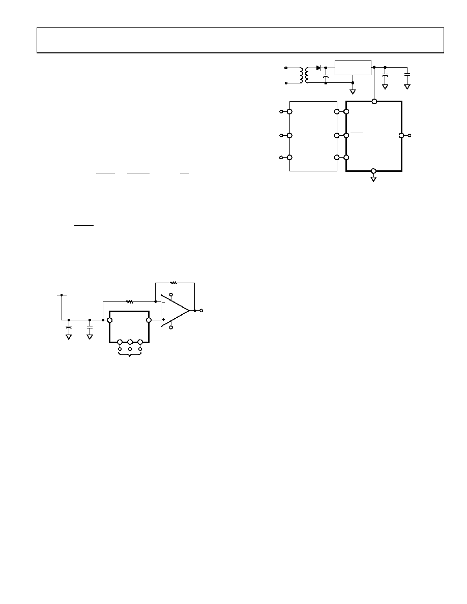
GALVANICALLY ISOLATED INTERFACE
In process control applications in industrial environments, it is
often necessary to use a galvanically isolated interface to protect
and isolate the controlling circuitry from any hazardous
common-mode voltages that might occur in the area where the
DAC is functioning. Isocouplers provide isolation in excess of
3 kV. The AD5624/AD5664 use a 3-wire serial logic interface,
so the ADuM130x 3-channel digital isolator provides the
required isolation (see Figure 41). The power supply to the part
also needs to be isolated, which is done by using a transformer.
On the DAC side of the transformer, a 5 V regulator provides
the 5 V supply required for the AD5624/AD5664.
0.1F
5V
REGULATOR
GND
DIN
SYNC
SCLK
POWER
10F
SDI
SCLK
DATA
AD5624/
AD5664
VOUT
VOB
VOA
VOC
VDD
V1C
V1B
V1A
ADuM1300
05
94
3-
0
44
Figure 41. AD5624/AD5664 with a Galvanically Isolated Interface
POWER SUPPLY BYPASSING AND GROUNDING
When accuracy is important in a circuit, it is helpful to consider
carefully the power supply and ground return layout on the
board. The printed circuit board containing the AD5624/
AD5664 should have separate analog and digital sections, each
having its own area of the board. If the AD5624/AD5664 is in a
system where other devices require an AGND-to-DGND
connection, the connection should be made at one point only.
This ground point should be as close as possible to the
AD5624/AD5664.
The power supply to the AD5624/AD5664 should be bypassed
with 10 μF and 0.1 μF capacitors. The capacitors should be
located as close as possible to the device, with the 0.1 μF capacitor
ideally right up against the device. The 10 μF capacitor is the
tantalum bead type. It is important that the 0.1 μF capacitor has
low effective series resistance (ESR) and effective series
inductance (ESI), for example, common ceramic types of
capacitors. This 0.1 μF capacitor provides a low impedance path
to ground for high frequencies caused by transient currents due
to internal logic switching.
The power supply line itself should have as large a trace as
possible to provide a low impedance path and to reduce glitch
effects on the supply line. Clocks and other fast switching
digital signals should be shielded from other parts of the board
by digital ground. Avoid crossover of digital and analog signals
if possible. When traces cross on opposite sides of the board,
ensure that they run at right angles to each other to reduce
feedthrough effects through the board. The best board layout
technique is the microstrip technique where the component
side of the board is dedicated to the ground plane only and the
signal traces are placed on the solder side. However, this is not
always possible with a 2-layer board.
相关PDF资料 |
PDF描述 |
|---|---|
| AD5667RBRMZ-2 | IC DAC NANO 16BIT DUAL 10-MSOP |
| AD5669RBRUZ-2 | IC DAC 16BIT I2C/SRL 16TSSOP |
| AD5680BRJZ-2500RL7 | IC DAC 18BIT 5V SOT23-8 |
| AD570JD | IC ADC 8BIT MONO W/CLK 18-CDIP |
| AD571JD | IC ADC 10BIT MONO W/CLK 18-CDIP |
相关代理商/技术参数 |
参数描述 |
|---|---|
| AD5664BCPZ-REEL7 | 功能描述:IC DAC NANO 16BIT QUAD 10-LFCSP RoHS:是 类别:集成电路 (IC) >> 数据采集 - 数模转换器 系列:nanoDAC™ 产品培训模块:Lead (SnPb) Finish for COTS Obsolescence Mitigation Program 标准包装:50 系列:- 设置时间:4µs 位数:12 数据接口:串行 转换器数目:2 电压电源:单电源 功率耗散(最大):- 工作温度:-40°C ~ 85°C 安装类型:表面贴装 封装/外壳:8-TSSOP,8-MSOP(0.118",3.00mm 宽) 供应商设备封装:8-uMAX 包装:管件 输出数目和类型:2 电压,单极 采样率(每秒):* 产品目录页面:1398 (CN2011-ZH PDF) |
| AD5664BRMZ | 功能描述:IC DAC NANO 16BIT QUAD 10-MSOP RoHS:是 类别:集成电路 (IC) >> 数据采集 - 数模转换器 系列:nanoDAC™ 产品培训模块:Lead (SnPb) Finish for COTS Obsolescence Mitigation Program 标准包装:50 系列:- 设置时间:4µs 位数:12 数据接口:串行 转换器数目:2 电压电源:单电源 功率耗散(最大):- 工作温度:-40°C ~ 85°C 安装类型:表面贴装 封装/外壳:8-TSSOP,8-MSOP(0.118",3.00mm 宽) 供应商设备封装:8-uMAX 包装:管件 输出数目和类型:2 电压,单极 采样率(每秒):* 产品目录页面:1398 (CN2011-ZH PDF) |
| AD5664BRMZ-REEL7 | 功能描述:IC DAC 16BIT QUAD 10-MSOP RoHS:是 类别:集成电路 (IC) >> 数据采集 - 数模转换器 系列:nanoDAC™ 标准包装:47 系列:- 设置时间:2µs 位数:14 数据接口:并联 转换器数目:1 电压电源:单电源 功率耗散(最大):55µW 工作温度:-40°C ~ 85°C 安装类型:表面贴装 封装/外壳:28-SSOP(0.209",5.30mm 宽) 供应商设备封装:28-SSOP 包装:管件 输出数目和类型:1 电流,单极;1 电流,双极 采样率(每秒):* |
| AD5664R | 制造商:AD 制造商全称:Analog Devices 功能描述:Quad, 12-/14-/16-Bit nanoDACs with 5 ppm/C On-Chip Reference |
| AD5664RBCBZ-3-RL7 | 制造商:Analog Devices 功能描述:QUAD3V16BITSPIDACWITHREFERENCE - Tape and Reel 制造商:Analog Devices 功能描述:IC DAC 16BIT QUAD 12WLCSP |
发布紧急采购,3分钟左右您将得到回复。