- 您现在的位置:买卖IC网 > PDF目录1979 > AD5664BCPZ-R2 (Analog Devices Inc)IC DAC NANO 16BIT QUAD 10-LFCSP PDF资料下载
参数资料
| 型号: | AD5664BCPZ-R2 |
| 厂商: | Analog Devices Inc |
| 文件页数: | 22/24页 |
| 文件大小: | 0K |
| 描述: | IC DAC NANO 16BIT QUAD 10-LFCSP |
| 产品培训模块: | Data Converter Fundamentals DAC Architectures |
| 标准包装: | 250 |
| 系列: | nanoDAC™ |
| 设置时间: | 4µs |
| 位数: | 16 |
| 数据接口: | DSP,MICROWIRE?,QSPI?,串行,SPI? |
| 转换器数目: | 4 |
| 电压电源: | 单电源 |
| 工作温度: | -40°C ~ 105°C |
| 安装类型: | 表面贴装 |
| 封装/外壳: | 10-WFDFN 裸露焊盘,CSP |
| 供应商设备封装: | 10-LFCSP-WD(3x3) |
| 包装: | 带卷 (TR) |
| 输出数目和类型: | 4 电压,单极;4 电压,双极 |
| 采样率(每秒): | 223k |
| 配用: | EVAL-AD5664REBZ-ND - BOARD EVALUATION FOR AD5664R |
AD5624/AD5664
Rev. 0 | Page 7 of 24
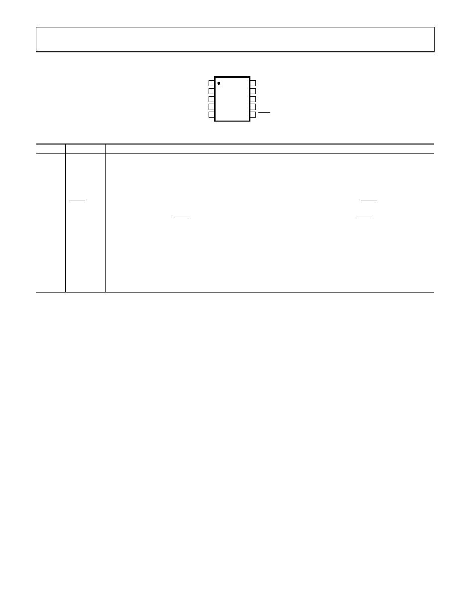
PIN CONFIGURATION AND FUNCTION DESCRIPTIONS
1
VOUTA
10
VREF
2
VOUTB
9
VDD
3
GND
8
DIN
4
VOUTC
7
SCLK
5
VOUTD
6
SYNC
AD5624/
AD5664
TOP VIEW
(Not to Scale)
0
59
43
-0
03
Figure 3. Pin Configuration
Table 6. Pin Function Descriptions
Pin No.
Mnemonic
Description
1
VOUTA
Analog Output Voltage from DAC A. The output amplifier has rail-to-rail operation.
2
VOUTB
Analog Output Voltage from DAC B. The output amplifier has rail-to-rail operation.
3
GND
Ground Reference Point for All Circuitry on the Part.
4
VOUTC
Analog Output Voltage from DAC C. The output amplifier has rail-to-rail operation.
5
VOUTD
Analog Output Voltage from DAC D. The output amplifier has rail-to-rail operation.
6
SYNC
Active Low Control Input. This is the frame synchronization signal for the input data. When SYNC goes low, it
powers on the SCLK and DIN buffers and enables the input shift register. Data is transferred in on the falling edges
of the next 24 clocks. If SYNC is taken high before the 24th falling edge, the rising edge of SYNC acts as an interrupt
and the write sequence is ignored by the device.
7
SCLK
Serial Clock Input. Data is clocked into the input shift register on the falling edge of the serial clock input. Data can
be transferred at rates up to 50 MHz.
8
DIN
Serial Data Input. This device has a 24-bit input shift register. Data is clocked into the register on the falling edge of
the serial clock input.
9
VDD
Power Supply Input. These parts can be operated from 2.7 V to 5.5 V. The supply should be decoupled with a 10 μF
capacitor in parallel with a 0.1 μF capacitor to GND.
10
VREF
Reference Voltage Input.
相关PDF资料 |
PDF描述 |
|---|---|
| AD5667RBRMZ-2 | IC DAC NANO 16BIT DUAL 10-MSOP |
| AD5669RBRUZ-2 | IC DAC 16BIT I2C/SRL 16TSSOP |
| AD5680BRJZ-2500RL7 | IC DAC 18BIT 5V SOT23-8 |
| AD570JD | IC ADC 8BIT MONO W/CLK 18-CDIP |
| AD571JD | IC ADC 10BIT MONO W/CLK 18-CDIP |
相关代理商/技术参数 |
参数描述 |
|---|---|
| AD5664BCPZ-REEL7 | 功能描述:IC DAC NANO 16BIT QUAD 10-LFCSP RoHS:是 类别:集成电路 (IC) >> 数据采集 - 数模转换器 系列:nanoDAC™ 产品培训模块:Lead (SnPb) Finish for COTS Obsolescence Mitigation Program 标准包装:50 系列:- 设置时间:4µs 位数:12 数据接口:串行 转换器数目:2 电压电源:单电源 功率耗散(最大):- 工作温度:-40°C ~ 85°C 安装类型:表面贴装 封装/外壳:8-TSSOP,8-MSOP(0.118",3.00mm 宽) 供应商设备封装:8-uMAX 包装:管件 输出数目和类型:2 电压,单极 采样率(每秒):* 产品目录页面:1398 (CN2011-ZH PDF) |
| AD5664BRMZ | 功能描述:IC DAC NANO 16BIT QUAD 10-MSOP RoHS:是 类别:集成电路 (IC) >> 数据采集 - 数模转换器 系列:nanoDAC™ 产品培训模块:Lead (SnPb) Finish for COTS Obsolescence Mitigation Program 标准包装:50 系列:- 设置时间:4µs 位数:12 数据接口:串行 转换器数目:2 电压电源:单电源 功率耗散(最大):- 工作温度:-40°C ~ 85°C 安装类型:表面贴装 封装/外壳:8-TSSOP,8-MSOP(0.118",3.00mm 宽) 供应商设备封装:8-uMAX 包装:管件 输出数目和类型:2 电压,单极 采样率(每秒):* 产品目录页面:1398 (CN2011-ZH PDF) |
| AD5664BRMZ-REEL7 | 功能描述:IC DAC 16BIT QUAD 10-MSOP RoHS:是 类别:集成电路 (IC) >> 数据采集 - 数模转换器 系列:nanoDAC™ 标准包装:47 系列:- 设置时间:2µs 位数:14 数据接口:并联 转换器数目:1 电压电源:单电源 功率耗散(最大):55µW 工作温度:-40°C ~ 85°C 安装类型:表面贴装 封装/外壳:28-SSOP(0.209",5.30mm 宽) 供应商设备封装:28-SSOP 包装:管件 输出数目和类型:1 电流,单极;1 电流,双极 采样率(每秒):* |
| AD5664R | 制造商:AD 制造商全称:Analog Devices 功能描述:Quad, 12-/14-/16-Bit nanoDACs with 5 ppm/C On-Chip Reference |
| AD5664RBCBZ-3-RL7 | 制造商:Analog Devices 功能描述:QUAD3V16BITSPIDACWITHREFERENCE - Tape and Reel 制造商:Analog Devices 功能描述:IC DAC 16BIT QUAD 12WLCSP |
发布紧急采购,3分钟左右您将得到回复。