- 您现在的位置:买卖IC网 > PDF目录8607 > AD5678BRUZ-1REEL7 (Analog Devices Inc)IC DAC 12/16BIT SPI/SRL 14TSSOP PDF资料下载
参数资料
| 型号: | AD5678BRUZ-1REEL7 |
| 厂商: | Analog Devices Inc |
| 文件页数: | 14/28页 |
| 文件大小: | 0K |
| 描述: | IC DAC 12/16BIT SPI/SRL 14TSSOP |
| 产品培训模块: | Data Converter Fundamentals DAC Architectures |
| 标准包装: | 1,000 |
| 设置时间: | 6µs |
| 位数: | 12,16 |
| 数据接口: | DSP,MICROWIRE?,QSPI?,串行,SPI? |
| 转换器数目: | 8 |
| 电压电源: | 单电源 |
| 工作温度: | -40°C ~ 105°C |
| 安装类型: | 表面贴装 |
| 封装/外壳: | 14-TSSOP(0.173",4.40mm 宽) |
| 供应商设备封装: | 14-TSSOP |
| 包装: | 带卷 (TR) |
| 输出数目和类型: | 8 电压,单极 |
| 采样率(每秒): | 95k |
第1页第2页第3页第4页第5页第6页第7页第8页第9页第10页第11页第12页第13页当前第14页第15页第16页第17页第18页第19页第20页第21页第22页第23页第24页第25页第26页第27页第28页
AD5678
Rev. C | Page 21 of 28
OUTPUT AMPLIFIER
The output buffer amplifier can generate rail-to-rail voltages on
its output, which gives an output range of 0 V to VDD. The
amplifier is capable of driving a load of 2 kΩ in parallel with
1,000 pF to GND. The source and sink capabilities of the output
is 1.5 V/μs with a to scale settling time of 10 μs.
SERIAL INTERFACE
The AD5678 has a 3-wire serial interface (SYNC, SCLK, and
DIN) that is compatible with SPI, QSPI, and MICROWIRE
interface standards as well as most DSPs. See
for a
timing diagram of a typical write sequence.
The write sequence begins by bringing the SYNC line low. Data
from the DIN line is clocked into the 32-bit shift register on the
falling edge of SCLK. The serial clock frequency can be as high
as 50 MHz, making the AD5678 compatible with high speed
DSPs. On the 32nd falling clock edge, the last data bit is clocked
in and the programmed function is executed, that is, a change
in DAC register contents and/or a change in the mode of
operation. At this stage, the SYNC line can be kept low or be
brought high. In either case, it must be brought high for a
minimum of 15 ns before the next write sequence so that a
falling edge of SYNC can initiate the next write sequence.
Because the SYNC buffer draws more current when VIN = 2 V
than it does when VIN = 0.8 V, SYNC should be idled low
between write sequences for even lower power operation of the
part. As is mentioned previously, however, SYNC must be
brought high again just before the next write sequence.
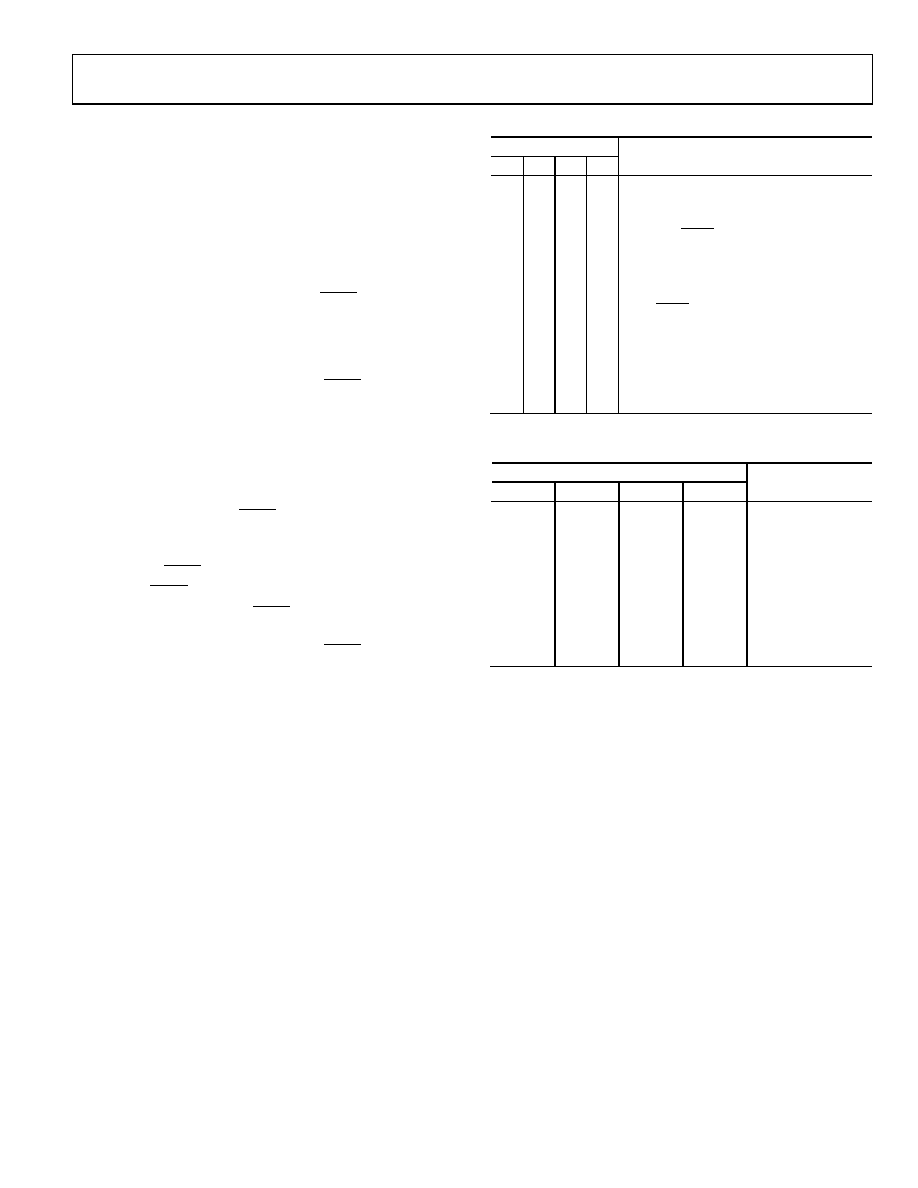
Table 7. Command Definitions
Command
C3
C2
C1
C0
Description
0
Write to Input Register n
0
1
Update DAC Register n
0
1
0
Write to Input Register n, update all
(software LDAC)
0
1
Write to and update DAC Channel n
0
1
0
Power down/power up DAC
0
1
0
1
Load clear code register
0
1
0
Load LDAC register
0
1
Reset (power-on reset)
1
0
Set up internal REF register
1
0
1
Reserved
–
Reserved
1
Reserved
Table 8. Address Commands
Address (n)
A3
A2
A1
A0
Selected DAC
Channel
0
DAC A (16 bits)
0
1
DAC B (16 bits)
0
1
0
DAC C (12 bits)
0
1
DAC D (12 bits)
0
1
0
DAC E (12 bits)
0
1
0
1
DAC F (12 bits)
0
1
0
DAC G (16 bits)
0
1
DAC H (16 bits)
1
All DACs
相关PDF资料 |
PDF描述 |
|---|---|
| VE-2T1-IV-F4 | CONVERTER MOD DC/DC 12V 150W |
| AD8307ARZ-REEL | IC AMP LOGARITHMIC 8SOIC |
| LTC6420IUDC-20#PBF | IC DIFF AMP/ADC DRIVER DL 20QFN |
| VE-2T1-IV-F3 | CONVERTER MOD DC/DC 12V 150W |
| LTC6421IUDC-20#TRPBF | IC ADC DRIVER DIFF 20-QFN |
相关代理商/技术参数 |
参数描述 |
|---|---|
| AD5678BRUZ-2 | 功能描述:IC DAC 12/16BIT SPI/SRL 16TSSOP RoHS:是 类别:集成电路 (IC) >> 数据采集 - 数模转换器 系列:- 标准包装:1 系列:- 设置时间:4.5µs 位数:12 数据接口:串行,SPI? 转换器数目:1 电压电源:单电源 功率耗散(最大):- 工作温度:-40°C ~ 125°C 安装类型:表面贴装 封装/外壳:8-SOIC(0.154",3.90mm 宽) 供应商设备封装:8-SOICN 包装:剪切带 (CT) 输出数目和类型:1 电压,单极;1 电压,双极 采样率(每秒):* 其它名称:MCP4921T-E/SNCTMCP4921T-E/SNRCTMCP4921T-E/SNRCT-ND |
| AD5678BRUZ-2REEL7 | 功能描述:IC DAC 12/16BIT SPI/SRL 16TSSOP RoHS:是 类别:集成电路 (IC) >> 数据采集 - 数模转换器 系列:- 产品培训模块:Data Converter Fundamentals DAC Architectures 标准包装:750 系列:- 设置时间:7µs 位数:16 数据接口:并联 转换器数目:1 电压电源:双 ± 功率耗散(最大):100mW 工作温度:0°C ~ 70°C 安装类型:表面贴装 封装/外壳:28-LCC(J 形引线) 供应商设备封装:28-PLCC(11.51x11.51) 包装:带卷 (TR) 输出数目和类型:1 电压,单极;1 电压,双极 采样率(每秒):143k |
| AD567JD | 功能描述:IC DAC 12BIT MONO 28-CDIP RoHS:否 类别:集成电路 (IC) >> 数据采集 - 数模转换器 系列:- 产品培训模块:Lead (SnPb) Finish for COTS Obsolescence Mitigation Program 标准包装:1,000 系列:- 设置时间:1µs 位数:8 数据接口:串行 转换器数目:8 电压电源:双 ± 功率耗散(最大):941mW 工作温度:0°C ~ 70°C 安装类型:表面贴装 封装/外壳:24-SOIC(0.295",7.50mm 宽) 供应商设备封装:24-SOIC W 包装:带卷 (TR) 输出数目和类型:8 电压,单极 采样率(每秒):* |
| AD567JD/+ | 制造商:Rochester Electronics LLC 功能描述:IC, MONO 12-BIT D/A CONV - Bulk |
| AD567KD | 功能描述:IC DAC 12BIT MONO 28-CDIP RoHS:否 类别:集成电路 (IC) >> 数据采集 - 数模转换器 系列:- 产品培训模块:Lead (SnPb) Finish for COTS Obsolescence Mitigation Program 标准包装:1,000 系列:- 设置时间:1µs 位数:8 数据接口:串行 转换器数目:8 电压电源:双 ± 功率耗散(最大):941mW 工作温度:0°C ~ 70°C 安装类型:表面贴装 封装/外壳:24-SOIC(0.295",7.50mm 宽) 供应商设备封装:24-SOIC W 包装:带卷 (TR) 输出数目和类型:8 电压,单极 采样率(每秒):* |
发布紧急采购,3分钟左右您将得到回复。