参数资料
| 型号: | AD5678BRUZ-2 |
| 厂商: | Analog Devices Inc |
| 文件页数: | 18/28页 |
| 文件大小: | 0K |
| 描述: | IC DAC 12/16BIT SPI/SRL 16TSSOP |
| 产品培训模块: | Data Converter Fundamentals DAC Architectures |
| 标准包装: | 1 |
| 设置时间: | 6µs |
| 位数: | 12,16 |
| 数据接口: | DSP,MICROWIRE?,QSPI?,串行,SPI? |
| 转换器数目: | 8 |
| 电压电源: | 单电源 |
| 工作温度: | -40°C ~ 105°C |
| 安装类型: | 表面贴装 |
| 封装/外壳: | 16-TSSOP(0.173",4.40mm 宽) |
| 供应商设备封装: | 16-TSSOP |
| 包装: | 管件 |
| 输出数目和类型: | 8 电压,单极 |
| 采样率(每秒): | 95k |
| 产品目录页面: | 784 (CN2011-ZH PDF) |
第1页第2页第3页第4页第5页第6页第7页第8页第9页第10页第11页第12页第13页第14页第15页第16页第17页当前第18页第19页第20页第21页第22页第23页第24页第25页第26页第27页第28页
AD5678
Rev. C | Page 25 of 28
LDAC FUNCTION
The outputs of all DACs can be updated simultaneously using
the hardware LDAC pin.
Synchronous LDAC: After new data is read, the DAC registers
are updated on the falling edge of the 32nd SCLK pulse. LDAC
can be permanently low or pulsed as in
.
Asynchronous LDAC: The outputs are not updated at the same
time that the input registers are written to. When LDAC goes low,
the DAC registers are updated with the contents of the input register.
Alternatively, the outputs of all DACs can be updated simulta-
neously using the software LDAC function by writing to Input
Register n and updating all DAC registers. Command 0011 is
reserved for this software LDAC function.
An LDAC register gives the user extra flexibility and control
over the hardware LDAC pin. This register allows the user to
select which combination of channels to simultaneously update
when the hardware LDAC pin is executed. Setting the LDAC bit
register to 0 for a DAC channel means that this channel’s update
is controlled by the LDAC pin. If this bit is set to 1, this channel
updates synchronously; that is, the DAC register is updated
after new data is read, regardless of the state of the LDAC pin. It
effectively sees the LDAC pin as being tied low. (See
for the
LDAC register mode of operation.) This flexibility is
useful in applications where the user wants to simultaneously
update select channels while the rest of the channels are
synchronously updating.
Writing to the DAC using command 0110 loads the 8-bit LDAC
register (DB7 to DB0). The default for each channel is 0; that is,
the LDAC pin works normally. Setting the bits to 1 means the
DAC channel is updated regardless of the state of the LDAC
pin. See
for the contents of the input shift register
during the load
LDAC register mode of operation.
POWER SUPPLY BYPASSING AND GROUNDING
When accuracy is important in a circuit, it is helpful to carefully
consider the power supply and ground return layout on the
board. The printed circuit board containing the AD5678 should
have separate analog and digital sections. If the AD5678 is in a
system where other devices require an AGND-to-DGND
connection, the connection should be made at one point only.
This ground point should be as close as possible to the AD5678.
The power supply to the AD5678 should be bypassed with 10 μF
and 0.1 μF capacitors. The capacitors should physically be as
close as possible to the device, with the 0.1 μF capacitor ideally
right up against the device. The 10 μF capacitors are the tantalum
bead type. It is important that the 0.1 μF capacitor has low effective
series resistance (ESR) and low effective series inductance (ESI),
such as is typical of common ceramic types of capacitors. This
0.1 μF capacitor provides a low impedance path to ground for
high frequencies caused by transient currents due to internal
logic switching.
The power supply line should have as large a trace as possible to
provide a low impedance path and reduce glitch effects on the
supply line. Clocks and other fast switching digital signals should
be shielded from other parts of the board by digital ground. Avoid
crossover of digital and analog signals if possible. When traces
cross on opposite sides of the board, ensure that they run at right
angles to each other to reduce feedthrough effects through the
board. The best board layout technique is the microstrip technique,
where the component side of the board is dedicated to the ground
plane only and the signal traces are placed on the solder side.
However, this is not always possible with a 2-layer board.
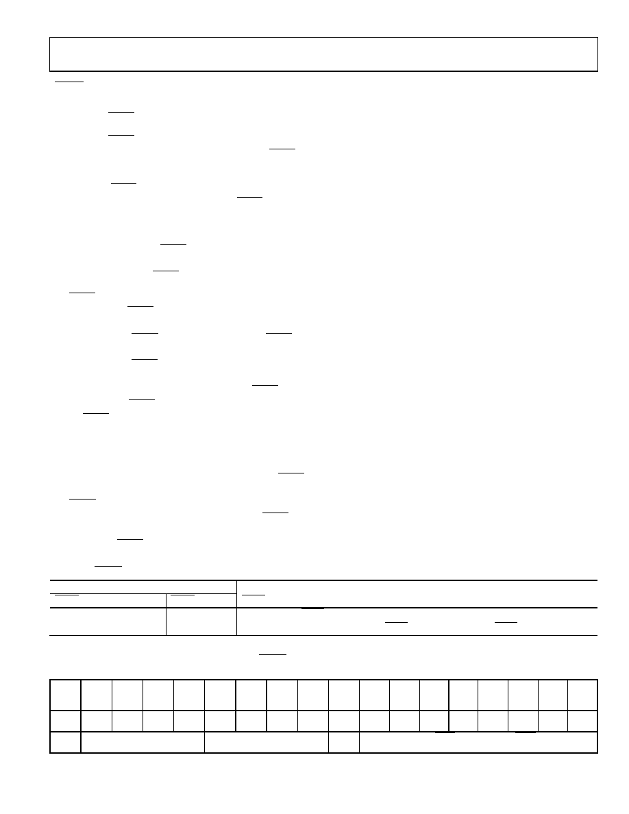
Table 15. LDAC Register
Load DAC Register
LDAC Bits (DB7 to DB0)
LDAC Pin
LDAC Operation
0
1/0
Determined by LDAC pin
1
X—don’t care
DAC channels update, overriding the LDAC pin. DAC channels see LDAC as 0.
Table 16. 32-Bit Input Shift Register Contents for LDAC Overwrite Function
MSB
LSB
DB31
to
DB28
DB27
DB26
DB25
DB24
DB23
DB22
DB21
DB20
DB19
to
DB8
DB7
DB6
DB5
DB4
DB3
DB2
DB1
DB0
X
0
1
0
X
DAC
H
DAC
G
DAC
F
DAC
E
DAC
D
DAC
C
DAC
B
DAC
A
Don’t
cares
Command bits (C3 to C0)
Address bits (A3 to A0)—
don’t cares
Don’t
cares
Setting LDAC bit to 1 overrides LDAC pin
相关PDF资料 |
PDF描述 |
|---|---|
| AD5735ACPZ | IC DAC QUAD VOLT CUR 64-LFCSP |
| AD5044BRUZ | IC DAC QUAD 14BIT SPI 16TSSOP |
| MS3454W24-22S | CONN RCPT 4POS JAM NUT W/SCKT |
| ADV7125JSTZ330 | IC DAC VIDEO 3CH 330MHZ 48LQFP |
| VE-21N-MY-F2 | CONVERTER MOD DC/DC 18.5V 50W |
相关代理商/技术参数 |
参数描述 |
|---|---|
| AD5678BRUZ-2REEL7 | 功能描述:IC DAC 12/16BIT SPI/SRL 16TSSOP RoHS:是 类别:集成电路 (IC) >> 数据采集 - 数模转换器 系列:- 产品培训模块:Data Converter Fundamentals DAC Architectures 标准包装:750 系列:- 设置时间:7µs 位数:16 数据接口:并联 转换器数目:1 电压电源:双 ± 功率耗散(最大):100mW 工作温度:0°C ~ 70°C 安装类型:表面贴装 封装/外壳:28-LCC(J 形引线) 供应商设备封装:28-PLCC(11.51x11.51) 包装:带卷 (TR) 输出数目和类型:1 电压,单极;1 电压,双极 采样率(每秒):143k |
| AD567JD | 功能描述:IC DAC 12BIT MONO 28-CDIP RoHS:否 类别:集成电路 (IC) >> 数据采集 - 数模转换器 系列:- 产品培训模块:Lead (SnPb) Finish for COTS Obsolescence Mitigation Program 标准包装:1,000 系列:- 设置时间:1µs 位数:8 数据接口:串行 转换器数目:8 电压电源:双 ± 功率耗散(最大):941mW 工作温度:0°C ~ 70°C 安装类型:表面贴装 封装/外壳:24-SOIC(0.295",7.50mm 宽) 供应商设备封装:24-SOIC W 包装:带卷 (TR) 输出数目和类型:8 电压,单极 采样率(每秒):* |
| AD567JD/+ | 制造商:Rochester Electronics LLC 功能描述:IC, MONO 12-BIT D/A CONV - Bulk |
| AD567KD | 功能描述:IC DAC 12BIT MONO 28-CDIP RoHS:否 类别:集成电路 (IC) >> 数据采集 - 数模转换器 系列:- 产品培训模块:Lead (SnPb) Finish for COTS Obsolescence Mitigation Program 标准包装:1,000 系列:- 设置时间:1µs 位数:8 数据接口:串行 转换器数目:8 电压电源:双 ± 功率耗散(最大):941mW 工作温度:0°C ~ 70°C 安装类型:表面贴装 封装/外壳:24-SOIC(0.295",7.50mm 宽) 供应商设备封装:24-SOIC W 包装:带卷 (TR) 输出数目和类型:8 电压,单极 采样率(每秒):* |
| AD567KD/+ | 制造商:Analog Devices 功能描述: |
发布紧急采购,3分钟左右您将得到回复。