参数资料
| 型号: | AD568KQ |
| 厂商: | Analog Devices Inc |
| 文件页数: | 4/14页 |
| 文件大小: | 0K |
| 描述: | IC DAC 12BIT HS MONO 35NS 24CDIP |
| 产品培训模块: | Data Converter Fundamentals DAC Architectures |
| 标准包装: | 1 |
| 设置时间: | 35ns |
| 位数: | 12 |
| 数据接口: | 并联 |
| 转换器数目: | 1 |
| 电压电源: | 双 ± |
| 工作温度: | 0°C ~ 70°C |
| 安装类型: | 通孔 |
| 封装/外壳: | 24-CDIP(0.300",7.62mm) |
| 供应商设备封装: | 24-CDIP |
| 包装: | 管件 |
| 输出数目和类型: | 1 电流,单极;1 电流,双极;1 电压,单极;1 电压,双极 |
| 采样率(每秒): | * |
AD568
REV. A
–12–
Circuit Details
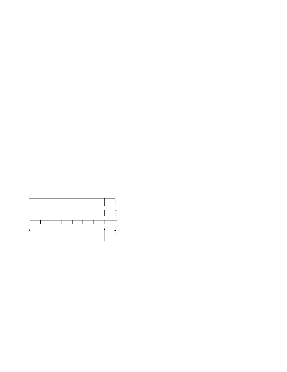
Figure 20 shows an approximate timing budget for the A/D con-
verter. If 12 cycles are to be completed in 1
s, approximately
80 ns is allowed for each cycle. Since the Schottky diodes clamp
the voltage of the summing junction, the DAC settling time ap-
proaches the current-settling value of 35 ns, and hence uses up
less than half the timing budget.
To maintain simplicity, a simple clock is used that runs at a
constant rate throughout the conversion, with a duty cycle of
approximately 90%. If absolute speed is worth the additional
complexity, the clock frequency can be increased as the conver-
sion progresses since the DAC must settle from increasingly
smaller steps.
When seeking a cycle time of less than 100 ns, the delays gener-
ated by the older generation SAR registers become problematic.
Newer, high speed SAR logic chips are becoming available in
the classic 2504 pinout that cuts the logic overhead in half. One
example of this is Zyrel’s ZR2504.
Finding a comparator capable of keeping up with this DAC ar-
rangement is fairly difficult: it must respond to an overdrive of
250
V (1 LSB) in less than 25 ns. Since no inexpensive com-
parator exists with these specs, special arrangements must be
made. The LT106 comparator provides relatively quick re-
sponse, but requires at least 5 mV of overdrive to maintain this
speed. A discrete preamplifier may be used to amplify the sum-
ming junction voltage to sufficiently overdrive the comparator.
Care must be exercised in the layout of the preamp/comparator
block to avoid introducing comparator instability with the
preamp’s additional gain.
10ns
35ns
15ns
10ns
0
10ns
20ns
30ns
40ns
50ns
60ns
70ns
80ns
CLOCK
PULSE
START OF NEXT
CLOCK CYCLE
LATCH COMPARATOR
START OF
CLOCK CYCLE
SAR
DELAY
DAC SETTLING
PREAMP
DELAY
COMPARATOR
DELAY
Figure 20. Typical Clock Cycle for a 1
s SAR A/D
Converter
HIGH-SPEED MULTIPLYING DAC
A powerful use for the AD568 is found in multiplying applica-
tions, where the DAC controls the amplitude of a high-speed
signal. Specifically, using the AD568 as the control voltage
input signal for the AD539 60 MHz analog multiplier and
AD5539 wideband op amp, a high-speed multiplying DAC can
be built.
In the application shown in Figure 21, the AD568 is used in a
buffered voltage output mode to generate the input to the
AD539’s control channel. The speed of the AD568 allows
oversampling of the control signal waveform voltage, thereby
providing increased spectral purity of the amplitude envelope
that modulates the analog input channels.
The AD568 is configured in the unbuffered unipolar output
mode. The internal 200
load resistor creates the 0-1 V FS
output signal, which is buffered and amplified to a 0-3 V range
suitable for the control channel of the AD539.
A 500
input impedance exists at Pin 1, the input channel. To
provide a buffer for the 0-1 V output signal from the AD568
looking into the impedance and to achieve the full-scale range,
the AD841, high-speed, fast settling op amp is included. The
gain of 3 is achieved with a 2 k
resistor configured in follower
mode with a 1 k
pot and 500 resistor. A 20 k pot with
connections to Pins 3, 4 and 12 is provided for offset trim.
The AD539 can accept two separate input signals, each with a
nominal full-scale voltage range of
±2 V. Each signal can then
be simultaneously controlled by the AD568 signal at the com-
mon input channels, Pins 11 and 14, applied to the AD5539 in
a subtracting configuration, provide the voltage output signal:
VOUT =
D
4096
×
VY1 –VY 2
2V
(0
≤D ≤4095)
For applications where only a single channel is involved, chan-
nel 2, VY2, is tied to ground. This provides:
VOUT =
D
4096
×
VY1
2V
(0
≤D ≤4095)
Some AD539 circuit details: The control amplifier compensa-
tion capacitor for Pin 2, CC, must have a minimum value of
300 pF to provide circuit stability. For improved bandwidth and
feedthrough, the feedthrough capacitor between Pins 1 and 2
should be 5-20% of CC. A Schottky diode at Pin 2 can improve
recovery time from small negative values of VX. Lead lengths
along the path of the high-speed signal from AD568 should be
kept at a minimum.
相关PDF资料 |
PDF描述 |
|---|---|
| AD569AD | IC DAC 16BIT MONO 28-CDIP |
| AD5700-1BCPZ-RL7 | IC HART MODEM LP INT OSC 24LFCSP |
| AD5726YRSZ-1REEL | IC DAC 12BIT QUAD SERIAL 20-SSOP |
| AD5754RBREZ-REEL7 | IC DAC 16BIT DSP/SRL 24TSSOP |
| AD5757ACPZ-REEL7 | IC DAC 16BIT QUAD IOUT 64LFCSP |
相关代理商/技术参数 |
参数描述 |
|---|---|
| AD568S | 制造商:AD 制造商全称:Analog Devices 功能描述:12-Bit Ultrahigh Speed Monolithic D/A Converter |
| AD568SE/883B | 制造商:Rochester Electronics LLC 功能描述:- Bulk 制造商:Analog Devices 功能描述: |
| AD568SQ | 功能描述:数模转换器- DAC IC MONO 12-BIT D/A CONV RoHS:否 制造商:Texas Instruments 转换器数量:1 DAC 输出端数量:1 转换速率:2 MSPs 分辨率:16 bit 接口类型:QSPI, SPI, Serial (3-Wire, Microwire) 稳定时间:1 us 最大工作温度:+ 85 C 安装风格:SMD/SMT 封装 / 箱体:SOIC-14 封装:Tube |
| AD568SQ/883B | 功能描述:数模转换器- DAC IC MONO 12-BIT RoHS:否 制造商:Analog Devices 转换器数量:4 DAC 输出端数量:4 转换速率: 分辨率:12 bit 接口类型:Serial (I2C) 稳定时间: 最大工作温度:+ 105 C 安装风格: 封装 / 箱体:TSSOP 封装:Reel |
| AD569 | 制造商:AD 制造商全称:Analog Devices 功能描述:16-Bit Monotonic Voltage Output D/A Converter |
发布紧急采购,3分钟左右您将得到回复。