参数资料
| 型号: | AD568KQ |
| 厂商: | Analog Devices Inc |
| 文件页数: | 9/14页 |
| 文件大小: | 0K |
| 描述: | IC DAC 12BIT HS MONO 35NS 24CDIP |
| 产品培训模块: | Data Converter Fundamentals DAC Architectures |
| 标准包装: | 1 |
| 设置时间: | 35ns |
| 位数: | 12 |
| 数据接口: | 并联 |
| 转换器数目: | 1 |
| 电压电源: | 双 ± |
| 工作温度: | 0°C ~ 70°C |
| 安装类型: | 通孔 |
| 封装/外壳: | 24-CDIP(0.300",7.62mm) |
| 供应商设备封装: | 24-CDIP |
| 包装: | 管件 |
| 输出数目和类型: | 1 电流,单极;1 电流,双极;1 电压,单极;1 电压,双极 |
| 采样率(每秒): | * |
AD568
REV. A
–4–
their glitch impulse. It is specified as the net area of the glitch in
nV-sec or pA-sec.
COMPLIANCE VOLTAGE: The range of allowable voltage at
the output of a current-output DAC which will not degrade the
accuracy of the output current.
SETTLING TIME: The time required for the output to reach
and remain within a specified error band about its final value,
measured from the digital input transition.
TIME – ns
0.8
0
250
50
OUTPUT
–
VOLTS
100
150
200
0.6
0.4
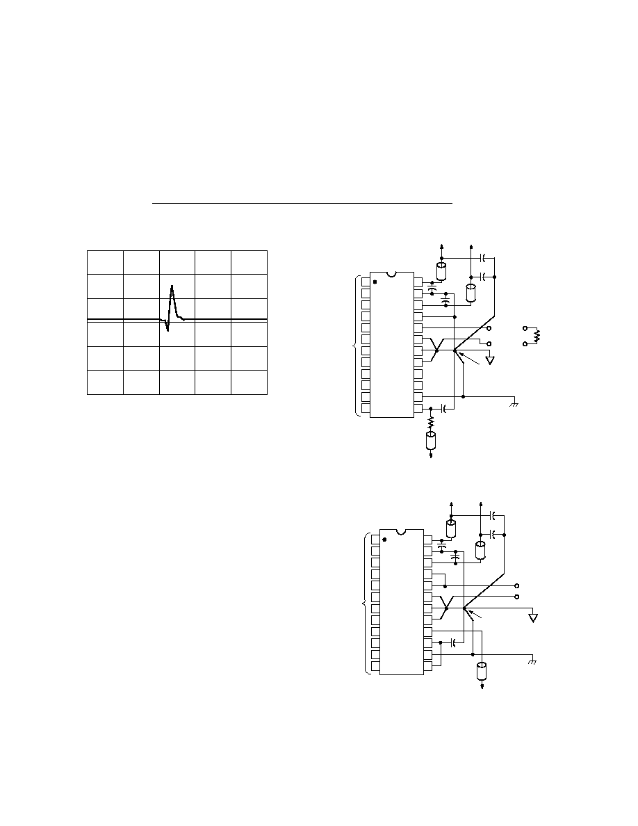
Figure 2. Glitch Impulse
Connecting the AD568
UNBUFFERED VOLTAGE OUTPUT
Unipolar Configuration
Figure 3 shows the AD568 configured to provide a unipolar 0 to
+1.024 V output range. In this mode, the bipolar offset termi-
nal, Pin 21, should be grounded if not used for offset trimming.
The nominal output impedance of the AD568 with Pin 19
grounded has been trimmed to 100
, ±1%. Other output im-
pedances can be generated with an external resistor, REXT, be-
tween Pins 19 and 20. An REXT equalling 300 will yield a
total output resistance of 75
, while an R
EXT of 100
will pro-
vide 50
of output resistance. Note that since the full-scale
output current of the DAC remains 10.24 mA, changing the
load impedance changes the unbuffered output voltage accord-
ingly. Settling time and full-scale range characteristics for these
load impedances are provided in the specifications table.
Bipolar Configuration
Figure 4 shows the connection scheme used to provide a bipolar
output voltage range of 1.024 V. The bipolar offset (–0.512 V)
occurs when all bits are OFF (00 . . . 00), bipolar zero (0 V) oc-
curs when the MSB is ON with all other bits OFF (10 . . . 00),
and full-scale minus 1 LSB (0.51175 V) is generated when all
bits are ON (11 . . . 11). Figure 5 shows an optional bipolar
mode with a 2.048 V range. The scale factor in this mode will
not be as accurate as the configuration shown in Figure 4, be-
cause the laser-trimmed resistor RL is not used.
13
16
15
14
24
23
22
21
20
19
18
17
12
11
10
9
8
1
2
3
4
7
6
5
AD568
+15V
REFCOM
–15V
IBPO
RL
ACOM
LCOM
SPAN
THCOM
VTH
IOUT
DIGITAL
INPUTS
0.2F
0.1F
–15V
+15V
ANALOG
GND PLANE
DIGITAL
GND PLANE
DIGITAL
SUPPLY
GROUND
100pF
RTH
1k
+5V
ANALOG
OUTPUT
REXT
(OPTIONAL)
FERRITE BEADS
STACKPOLE 57-1392
OR
AMIDON FB-43B-101
OR EQUIVALENT
NC
ANALOG
SUPPLY GROUND
Figure 3. Unipolar Output Unbuffered 0 V to +1.024 V
13
16
15
14
24
23
22
21
20
19
18
17
12
11
10
9
8
1
2
3
4
7
6
5
AD568
+15V
REFCOM
–15V
IBPO
RL
ACOM
LCOM
SPAN
THCOM
VTH
IOUT
DIGITAL
INPUTS
0.2F
0.1F
–15V
+15V
ANALOG
GND PLANE
DIGITAL
GND PLANE
DIGITAL
SUPPLY
GROUND
100pF
+5V
ANALOG
OUTPUT
ANALOG
SUPPLY
GROUND
Figure 4. Bipolar Output Unbuffered
±0.512 V
Figure 4 also demonstrates how the internal span resistor may
be used to bias the VTH pin (Pin 13) from a 5 V supply. This
eliminates the requirement for an external RTH in applications
that do not require the precision span resistor.
BIPOLAR ZERO ERROR: The deviation of the analog output
from the ideal half-scale output of 0 V (or 0 mA) for bipolar
mode when only the MSB is on (100 . . .00) is called bipolar
zero error.
GAIN ERROR: The difference between the ideal and actual
output span of FS –1 LSB, expressed in % of FS, or LSB, when
all bits are on.
GLITCH IMPULSE: Asymmetrical switching times in a DAC
give rise to undesired output transients which are quantified by
相关PDF资料 |
PDF描述 |
|---|---|
| AD569AD | IC DAC 16BIT MONO 28-CDIP |
| AD5700-1BCPZ-RL7 | IC HART MODEM LP INT OSC 24LFCSP |
| AD5726YRSZ-1REEL | IC DAC 12BIT QUAD SERIAL 20-SSOP |
| AD5754RBREZ-REEL7 | IC DAC 16BIT DSP/SRL 24TSSOP |
| AD5757ACPZ-REEL7 | IC DAC 16BIT QUAD IOUT 64LFCSP |
相关代理商/技术参数 |
参数描述 |
|---|---|
| AD568S | 制造商:AD 制造商全称:Analog Devices 功能描述:12-Bit Ultrahigh Speed Monolithic D/A Converter |
| AD568SE/883B | 制造商:Rochester Electronics LLC 功能描述:- Bulk 制造商:Analog Devices 功能描述: |
| AD568SQ | 功能描述:数模转换器- DAC IC MONO 12-BIT D/A CONV RoHS:否 制造商:Texas Instruments 转换器数量:1 DAC 输出端数量:1 转换速率:2 MSPs 分辨率:16 bit 接口类型:QSPI, SPI, Serial (3-Wire, Microwire) 稳定时间:1 us 最大工作温度:+ 85 C 安装风格:SMD/SMT 封装 / 箱体:SOIC-14 封装:Tube |
| AD568SQ/883B | 功能描述:数模转换器- DAC IC MONO 12-BIT RoHS:否 制造商:Analog Devices 转换器数量:4 DAC 输出端数量:4 转换速率: 分辨率:12 bit 接口类型:Serial (I2C) 稳定时间: 最大工作温度:+ 105 C 安装风格: 封装 / 箱体:TSSOP 封装:Reel |
| AD569 | 制造商:AD 制造商全称:Analog Devices 功能描述:16-Bit Monotonic Voltage Output D/A Converter |
发布紧急采购,3分钟左右您将得到回复。