参数资料
| 型号: | AD569JN |
| 厂商: | Analog Devices Inc |
| 文件页数: | 3/12页 |
| 文件大小: | 0K |
| 描述: | IC DAC 16BIT MONO 28-DIP |
| 产品培训模块: | Data Converter Fundamentals DAC Architectures |
| 标准包装: | 13 |
| 设置时间: | 4µs |
| 位数: | 16 |
| 数据接口: | 并联 |
| 转换器数目: | 1 |
| 电压电源: | 双 ± |
| 工作温度: | 0°C ~ 70°C |
| 安装类型: | 通孔 |
| 封装/外壳: | 28-DIP(0.600",15.24mm) |
| 供应商设备封装: | 28-PDIP |
| 包装: | 管件 |
| 输出数目和类型: | 1 电压,单极;1 电压,双极 |
| 采样率(每秒): | * |
AD569
REV. A
–11–
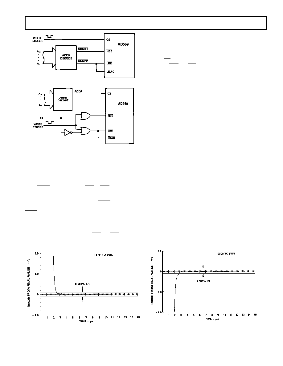
a. Simple Interface
b. Fast Interface
Figure 20. 8-Bit Microprocessor Interface
8-Bit Microprocessor Interfaces
Since 8-bit microprocessors require two write cycles to provide
the AD569’s 16-bit input, the DAC register must be utilized. It
is most often loaded as the second byte enters the first rank of
latches. This synchronous load method, shown in Figure 20, re-
quires LDAC to be tied to either LBE or HBE, depending upon
the byte loading sequence. In either case, the propagation delay
through the first rank gives rise to longer timing requirements as
shown in Figure 2. If the DAC register (LDAC) is controlled
separately using a third write cycle, the minimum write pulse on
LDAC
is 70 ns, as shown in Figure 1.
Two basic methods exist for interfacing the AD569 to an 8-bit
microprocessor’s address and control buses. In either case, at
least one address line is needed to differentiate between the up-
per and lower bytes of the first rank (HBE and LBE). The sim-
plest method involves applying the two addresses directly to
HBE
and LBE and strobing the data using CS as shown in Fig-
ure 20a. However, the minimum pulse width on CS is 70 ns
with a minimum data setup time of 60 ns. If operation with a
shorter pulse width is required, the base address should be ap-
plied to CS with an address line gated with the strobe signal to
supply the HBE and LBE inputs (see Figure 20b). However,
since the write pulse sees a propagation delay, the data still must
remain valid at least 20 ns after the rising edge of the delayed
write pulse.
OUTPUT SETTLING
The AD569’s output buffer amplifier typically settles to within
±0.001% FS of its final value in 3 s for a 10 V step. Figure 21
shows settling for negative and positive full-scale steps with no
load applied. Capable of sourcing or sinking 5 mA, the output
buffer can also drive loads of 1 k
and 1000 pF without loss of
stability. Typical settling to 0.001% under these worst-case con-
ditions is 4
s, and is guaranteed to be a maximum of 6 s. The
plots of Figure 21 were generated using the settling test proce-
dure developed specifically for the AD569.
Subranging 16-Bit ADC
The subranging ADC shown in Figure 22 completes a conver-
sion in less than 20
s, including the sample-hold amplifier’s
sample time. The sample-hold amplifier is allocated 5
s to
settle to 16 bits.
Before the first flash, the analog input signal is routed through
the AD630 at a gain of +1. The lower AD7820 quantizes the
signal to the 8-bit level within 1.4
s, and the 8-bit result is
routed to the AD569 via a digital latch which holds the 8-bit
word for the AD569 and the output logic.
The AD569’s reference polarity is reversed so that a full-scale
output is –5 V and zero scale is 0 V, thereby subtracting an 8-bit
approximation from the original sampled signal. The residue
from the analog subtraction is then quantized by the second 8-
bit flash conversion to recover the 8 LSBs. Even though only the
AD569’s upper 8 MSBs are used, the AD569’s accuracy de-
fines the A/D converter’s overall accuracy. Any errors are di-
rectly reflected in the output.
a. Turn-On Settling
b. Turn-Off Settling
Figure 21. Full-Scale Output Settling
相关PDF资料 |
PDF描述 |
|---|---|
| AD5570BRS | IC DAC 16BIT SERIAL IN 16SSOP |
| AD7547CQ | IC DAC 12BIT DUAL LC2MOS 24-CDIP |
| VI-26W-IV | CONVERTER MOD DC/DC 5.5V 150W |
| VI-26V-IV | CONVERTER MOD DC/DC 5.8V 150W |
| AD7834AR | IC DAC 14BIT QUAD SRL 28-SOIC |
相关代理商/技术参数 |
参数描述 |
|---|---|
| AD569JN | 制造商:Analog Devices 功能描述:Digital/Analog Converter IC Interface Ty |
| AD569JNZ | 功能描述:IC DAC 16BIT MONO 28-DIP RoHS:是 类别:集成电路 (IC) >> 数据采集 - 数模转换器 系列:- 标准包装:1 系列:- 设置时间:4.5µs 位数:12 数据接口:串行,SPI? 转换器数目:1 电压电源:单电源 功率耗散(最大):- 工作温度:-40°C ~ 125°C 安装类型:表面贴装 封装/外壳:8-SOIC(0.154",3.90mm 宽) 供应商设备封装:8-SOICN 包装:剪切带 (CT) 输出数目和类型:1 电压,单极;1 电压,双极 采样率(每秒):* 其它名称:MCP4921T-E/SNCTMCP4921T-E/SNRCTMCP4921T-E/SNRCT-ND |
| AD569JNZ | 制造商:Analog Devices 功能描述:D/A Converter (D-A) IC |
| AD569JP | 功能描述:IC DAC 16BIT MONO NON-LIN 28PLCC RoHS:否 类别:集成电路 (IC) >> 数据采集 - 数模转换器 系列:- 产品培训模块:Lead (SnPb) Finish for COTS Obsolescence Mitigation Program 标准包装:1,000 系列:- 设置时间:1µs 位数:8 数据接口:串行 转换器数目:8 电压电源:双 ± 功率耗散(最大):941mW 工作温度:0°C ~ 70°C 安装类型:表面贴装 封装/外壳:24-SOIC(0.295",7.50mm 宽) 供应商设备封装:24-SOIC W 包装:带卷 (TR) 输出数目和类型:8 电压,单极 采样率(每秒):* |
| AD569JP-REEL | 功能描述:IC DAC 16BIT MONO NON-LIN 28PLCC RoHS:否 类别:集成电路 (IC) >> 数据采集 - 数模转换器 系列:- 产品培训模块:Lead (SnPb) Finish for COTS Obsolescence Mitigation Program 标准包装:1,000 系列:- 设置时间:1µs 位数:8 数据接口:串行 转换器数目:8 电压电源:双 ± 功率耗散(最大):941mW 工作温度:0°C ~ 70°C 安装类型:表面贴装 封装/外壳:24-SOIC(0.295",7.50mm 宽) 供应商设备封装:24-SOIC W 包装:带卷 (TR) 输出数目和类型:8 电压,单极 采样率(每秒):* |
发布紧急采购,3分钟左右您将得到回复。