参数资料
| 型号: | AD569JN |
| 厂商: | Analog Devices Inc |
| 文件页数: | 9/12页 |
| 文件大小: | 0K |
| 描述: | IC DAC 16BIT MONO 28-DIP |
| 产品培训模块: | Data Converter Fundamentals DAC Architectures |
| 标准包装: | 13 |
| 设置时间: | 4µs |
| 位数: | 16 |
| 数据接口: | 并联 |
| 转换器数目: | 1 |
| 电压电源: | 双 ± |
| 工作温度: | 0°C ~ 70°C |
| 安装类型: | 通孔 |
| 封装/外壳: | 28-DIP(0.600",15.24mm) |
| 供应商设备封装: | 28-PDIP |
| 包装: | 管件 |
| 输出数目和类型: | 1 电压,单极;1 电压,双极 |
| 采样率(每秒): | * |
AD569
REV. A
–6–
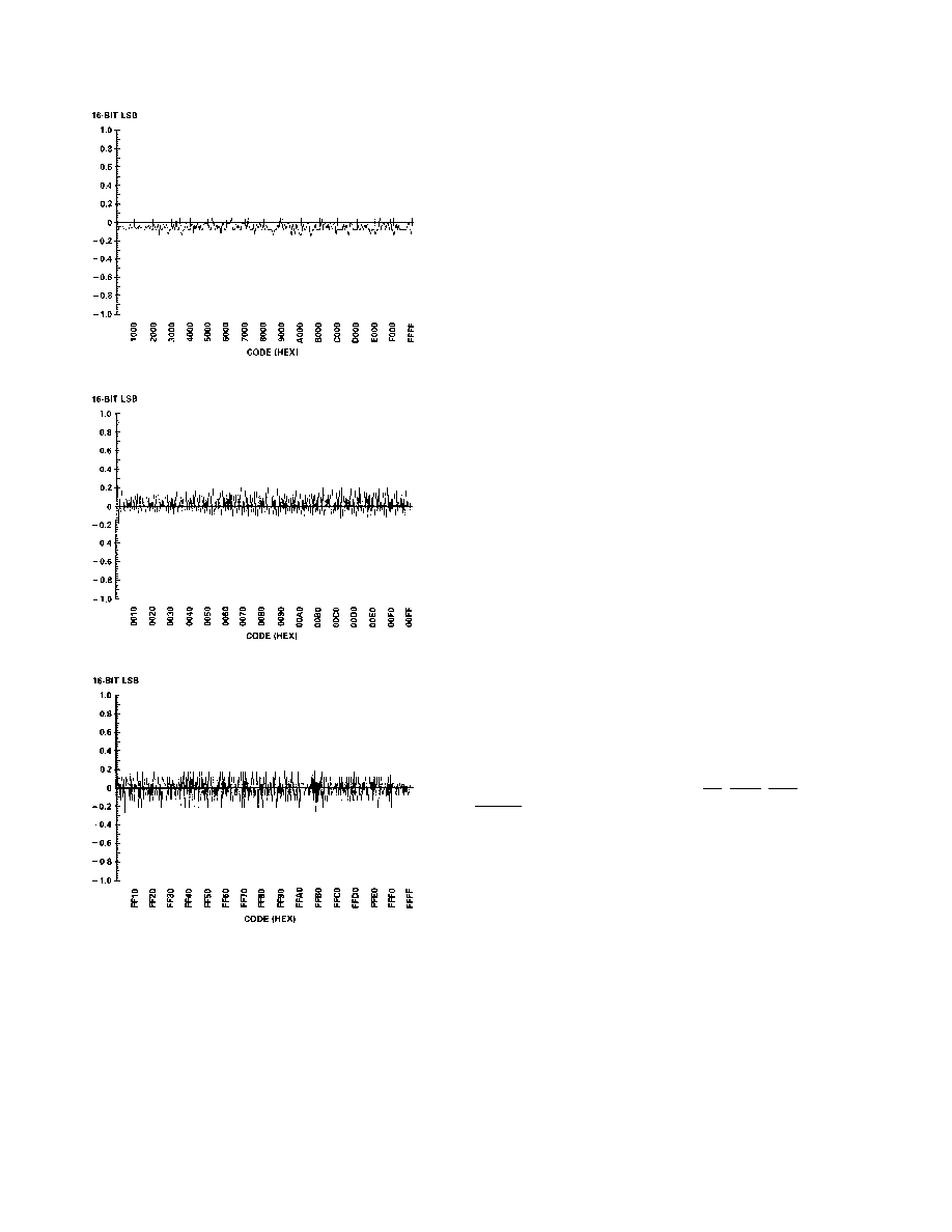
Figure 5. Typical DNL at Segment Boundary Transitions
a. Segment 1
b. Segment 256
Figure 6. Typical DNL Within Segments
MULTIPLYING FEEDTHROUGH ERROR: This is the error
due to capacitive feedthrough from the reference to the output
with the input registers loaded with all zeroes.
FULL-SCALE ERROR: The AD569’s voltage dividing archi-
tecture gives rise to a fixed full-scale error which is independent
of the reference voltage. This error is trimmed by adjusting the
voltage applied to the +VREF terminals.
DIGITAL-TO-ANALOG GLITCH IMPULSE: The charge in-
jected into the analog output when a new input is latched into
the DAC register gives rise to the Digital-to-Analog Glitch
Impulse.
Glitches can be due to either time skews between the input bits
or charge injection from the internal switches. Glitch Impulse
for the AD569 is mainly due to charge injection, and is mea-
sured with the reference connections tied to ground. It is speci-
fied as the area of the glitch in nV-secs.
TOTAL ERROR: The worst-case Total Error is the sum of the
fixed full-scale and offset errors and the linearity error.
POWER SUPPLY AND REFERENCE VOLTAGE RANGES
The AD569 is specified for operation with
±12 volt power
supplies. With
±10% power supply tolerances, the maximum
reference voltage range is
±5 volts. Reference voltages up to
±6 volts can be used but linearity will degrade if the supplies
approach their lower limits of
±10.8 volts (12 volts - 10%).
If
±12 volt power supplies are unavailable in the system, several
alternative schemes may be used to obtain the needed supply
voltages. For example, in a system with
±15 V supplies, a single
Zener diode can be used to reduce one of the supplies to 9 volts
with the remaining one left at 15 volts. Figure 7a illustrates this
scheme. A 1N753A or equivalent diode is an appropriate choice
for the task. Asymmetrical power supplies can be used since the
AD569’s output is referenced to –VREF only and thus floats
relative to logic ground (GND, Pin 18). Assuming a worst-case
±1.5 volt tolerance on both supplies (10% of 15 volts), the
maximum reference voltage ranges would be +6 and –2 volts for
+VS = +15 V and VS = –9 V, and +2 to –8 volts for +VS = 9 V
and –VS = –15 V .
Alternately, two 3 V Zener diodes or voltage regulators can be
used to drop each
±15 volt supply to ±12 volts, respectively. In
Figure 7b, 1N746A diodes are a good choice for this task.
A third method may be used if both
±15 volt and ±5 volt sup-
plies are available. Figure 7c shows this approach. A combina-
tion of +VS = +15 V and –VS = –5 V can support a reference
range of 0 to 6 volts, while supplies of +VS = +5 V and –VS =
–15 V can support a reference range of 0 to –8 volts. Again,
10% power supply tolerances are assumed.
NOTE: Operation with +VS = +5 V alters the input latches’ op-
erating conditions causing minimum write pulse widths to ex-
tend to 1
s or more. Control signals CS, HBE, LBE, and
LDAC
should, therefore, be tied low to render the latches trans-
parent.
No timing problems exist with operation at +VS = 9 V and
–VS = –15 V. However, 10% tolerances on these supplies gener-
ate a worst-case condition at –VS = –16.5 V and +VS = +7.5 V
(assuming +VS is derived from a +15 V supply). Under these
conditions, write pulse widths can stretch to 200 ns with similar
degradation of data setup and hold times. However,
±0.75 V
tolerances (
±5%) yield minimal effects on digital timing with
write pulse widths remaining below 100 ns.
Finally, Figure 7d illustrates the use of the combination of an
AD588 and AD569 in a system with
±15 volt supplies. As
shown, the AD588 is connected to provide
±5 V to the refer-
ence inputs of the AD569. It is doing double-duty by simulta-
neously regulating the supply voltages for the AD569 through
the use of the level shifting Zeners and transistors. This scheme
utilizes the capability of the outputs of the AD588 to source as
well as sink current. Two other benefits are realized by using
this approach. The first is that the AD569 is no longer directly
connected to the system power supplies. Output sensitivity to
variations in those supplies is, therefore, eliminated. The second
相关PDF资料 |
PDF描述 |
|---|---|
| AD5570BRS | IC DAC 16BIT SERIAL IN 16SSOP |
| AD7547CQ | IC DAC 12BIT DUAL LC2MOS 24-CDIP |
| VI-26W-IV | CONVERTER MOD DC/DC 5.5V 150W |
| VI-26V-IV | CONVERTER MOD DC/DC 5.8V 150W |
| AD7834AR | IC DAC 14BIT QUAD SRL 28-SOIC |
相关代理商/技术参数 |
参数描述 |
|---|---|
| AD569JN | 制造商:Analog Devices 功能描述:Digital/Analog Converter IC Interface Ty |
| AD569JNZ | 功能描述:IC DAC 16BIT MONO 28-DIP RoHS:是 类别:集成电路 (IC) >> 数据采集 - 数模转换器 系列:- 标准包装:1 系列:- 设置时间:4.5µs 位数:12 数据接口:串行,SPI? 转换器数目:1 电压电源:单电源 功率耗散(最大):- 工作温度:-40°C ~ 125°C 安装类型:表面贴装 封装/外壳:8-SOIC(0.154",3.90mm 宽) 供应商设备封装:8-SOICN 包装:剪切带 (CT) 输出数目和类型:1 电压,单极;1 电压,双极 采样率(每秒):* 其它名称:MCP4921T-E/SNCTMCP4921T-E/SNRCTMCP4921T-E/SNRCT-ND |
| AD569JNZ | 制造商:Analog Devices 功能描述:D/A Converter (D-A) IC |
| AD569JP | 功能描述:IC DAC 16BIT MONO NON-LIN 28PLCC RoHS:否 类别:集成电路 (IC) >> 数据采集 - 数模转换器 系列:- 产品培训模块:Lead (SnPb) Finish for COTS Obsolescence Mitigation Program 标准包装:1,000 系列:- 设置时间:1µs 位数:8 数据接口:串行 转换器数目:8 电压电源:双 ± 功率耗散(最大):941mW 工作温度:0°C ~ 70°C 安装类型:表面贴装 封装/外壳:24-SOIC(0.295",7.50mm 宽) 供应商设备封装:24-SOIC W 包装:带卷 (TR) 输出数目和类型:8 电压,单极 采样率(每秒):* |
| AD569JP-REEL | 功能描述:IC DAC 16BIT MONO NON-LIN 28PLCC RoHS:否 类别:集成电路 (IC) >> 数据采集 - 数模转换器 系列:- 产品培训模块:Lead (SnPb) Finish for COTS Obsolescence Mitigation Program 标准包装:1,000 系列:- 设置时间:1µs 位数:8 数据接口:串行 转换器数目:8 电压电源:双 ± 功率耗散(最大):941mW 工作温度:0°C ~ 70°C 安装类型:表面贴装 封装/外壳:24-SOIC(0.295",7.50mm 宽) 供应商设备封装:24-SOIC W 包装:带卷 (TR) 输出数目和类型:8 电压,单极 采样率(每秒):* |
发布紧急采购,3分钟左右您将得到回复。