参数资料
| 型号: | AD569JP |
| 厂商: | Analog Devices Inc |
| 文件页数: | 2/12页 |
| 文件大小: | 0K |
| 描述: | IC DAC 16BIT MONO NON-LIN 28PLCC |
| 产品培训模块: | Data Converter Fundamentals DAC Architectures |
| 标准包装: | 1 |
| 设置时间: | 4µs |
| 位数: | 16 |
| 数据接口: | 并联 |
| 转换器数目: | 1 |
| 电压电源: | 双 ± |
| 工作温度: | 0°C ~ 70°C |
| 安装类型: | 表面贴装 |
| 封装/外壳: | 28-LCC(J 形引线) |
| 供应商设备封装: | 28-PLCC(11.51x11.51) |
| 包装: | 管件 |
| 输出数目和类型: | 1 电压,单极;1 电压,双极 |
| 采样率(每秒): | * |
AD569
REV. A
–10–
Table I. AD569 Truth Table
CS
HBE
LBE
LDAC
OPERATION
1
X
No Operation
X
1
No Operation
0
1
Enable 8 MSBs of First Rank
0
1
0
1
Enable 8 LSBs of First Rank
0
1
0
Enable 16-Bit DAC Register
0
All Latches Transparent
All four control inputs latches are level-triggered and active low.
When the DAC register is loaded directly from a bus, the data at
the digital inputs will be reflected in the output any time CS,
LDAC
, LBE and HBE are low. Should this not be the desired
case, bring LDAC (or HBE or LBE) high before changing the
data. Alternately, use a second write cycle to transfer the data to
the DAC register or delay the write strobe pulse until the appro-
priate data is valid. Be sure to observe the appropriate data
setup and hold times (see Timing Characteristics).
Whenever possible, the write strobe signal should be applied to
HBE
and LBE with the AD569’s decoded address applied to
CS
. A minimum pulse width of 60 ns at HBE and LBE allows
the AD569 to interface to the fastest microprocessors. Actually,
data can be latched with narrower pulses, but the data setup and
hold times must be lengthened.
16-Bit Microprocessor Interfaces
Since 16-bit microprocessors supply the AD569’s complete 16-
bit input in one write cycle, the DAC register is often unneces-
sary. If so, it should be made transparent by grounding LDAC.
The DAC’s decoded address should be applied to CS, with the
write strobe applied to HBE and LBE as shown in the 68000 in-
terface in Figure 19.
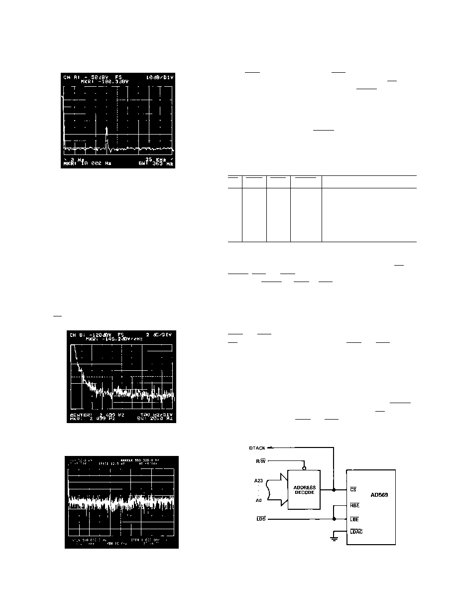
Figure 19. AD569/68000 Interface
DIGITAL CIRCUIT CONNECTIONS
The AD569’s truth table appears in Table I. The High Byte En-
able (HBE) and Low Byte Enable (LBE) inputs load the upper
and lower bytes of the 16-bit input when Chip Select (CS) is
valid (low). A similar strobe to Load DAC (LDAC) loads the
16-bit input into the DAC register and completes the DAC up-
date. The DAC register can either be loaded with a separate
write cycle or synchronously with either of the 8-bit registers in
the first rank. A simultaneous update of several AD569s can be
achieved by controlling their LDAC inputs with a single control
signal.
under worst-case conditions (hex input code 0000), feedthrough
remains below –100 dB at ac reference frequencies up to 10 kHz.
Figure 16. Multiplying Feedthrough
BYPASSING AND GROUNDING RULES
It is generally considered good engineering practice to use bypass
capacitors on the device supply voltage pins and to insert small
valued resistors in the supply lines to provide a measure of decou-
pling between various circuits in a system. For the AD569, bypass
capacitors of at least 4.7
F and series resistors of 10 are recom-
mended. The supply voltage pins should be decoupled to Pin 18.
NOISE
In high-resolution systems, noise is often the limiting factor. A
16-bit DAC with a 10 volt span has an LSB size of 152
V
(–96 dB). Therefore, the noise floor must remain below this
level in the frequency ranges of interest. The AD569’s noise
spectral density is shown in Figures 17 and 18. The lowband
noise spectrum in Figure 17 shows the 1/f corner frequency at
1.2 kHz and Figure 18 shows the wideband noise to be below
40 nV/
Hz
.
Figure 17. Lowband Noise Spectrum
Figure 18. Wideband Noise Spectrum
相关PDF资料 |
PDF描述 |
|---|---|
| VE-B5T-MX-S | CONVERTER MOD DC/DC 6.5V 75W |
| VE-B5R-MX-S | CONVERTER MOD DC/DC 7.5V 75W |
| LTC1821-1AIGW#TRPBF | IC D/A CONV 16BIT PRECISE 36SSOP |
| LTC1821AIGW#TR | IC D/A CONV 16BIT PRECISE 36SSOP |
| VE-B5P-MX-S | CONVERTER MOD DC/DC 13.8V 75W |
相关代理商/技术参数 |
参数描述 |
|---|---|
| AD569JP-REEL | 功能描述:IC DAC 16BIT MONO NON-LIN 28PLCC RoHS:否 类别:集成电路 (IC) >> 数据采集 - 数模转换器 系列:- 产品培训模块:Lead (SnPb) Finish for COTS Obsolescence Mitigation Program 标准包装:1,000 系列:- 设置时间:1µs 位数:8 数据接口:串行 转换器数目:8 电压电源:双 ± 功率耗散(最大):941mW 工作温度:0°C ~ 70°C 安装类型:表面贴装 封装/外壳:24-SOIC(0.295",7.50mm 宽) 供应商设备封装:24-SOIC W 包装:带卷 (TR) 输出数目和类型:8 电压,单极 采样率(每秒):* |
| AD569JPZ | 功能描述:IC DAC 16BIT MONO NON-LIN 28PLCC RoHS:是 类别:集成电路 (IC) >> 数据采集 - 数模转换器 系列:- 产品培训模块:Lead (SnPb) Finish for COTS Obsolescence Mitigation Program 标准包装:50 系列:- 设置时间:4µs 位数:12 数据接口:串行 转换器数目:2 电压电源:单电源 功率耗散(最大):- 工作温度:-40°C ~ 85°C 安装类型:表面贴装 封装/外壳:8-TSSOP,8-MSOP(0.118",3.00mm 宽) 供应商设备封装:8-uMAX 包装:管件 输出数目和类型:2 电压,单极 采样率(每秒):* 产品目录页面:1398 (CN2011-ZH PDF) |
| AD569JPZ-REEL | 功能描述:IC DAC 16BIT MONO NON-LIN 28PLCC RoHS:是 类别:集成电路 (IC) >> 数据采集 - 数模转换器 系列:- 产品培训模块:Lead (SnPb) Finish for COTS Obsolescence Mitigation Program 标准包装:1,000 系列:- 设置时间:1µs 位数:8 数据接口:串行 转换器数目:8 电压电源:双 ± 功率耗散(最大):941mW 工作温度:0°C ~ 70°C 安装类型:表面贴装 封装/外壳:24-SOIC(0.295",7.50mm 宽) 供应商设备封装:24-SOIC W 包装:带卷 (TR) 输出数目和类型:8 电压,单极 采样率(每秒):* |
| AD569KN | 功能描述:IC DAC 16BIT MONO NON-LIN 28-DIP RoHS:否 类别:集成电路 (IC) >> 数据采集 - 数模转换器 系列:- 产品培训模块:Lead (SnPb) Finish for COTS Obsolescence Mitigation Program 标准包装:1,000 系列:- 设置时间:1µs 位数:8 数据接口:串行 转换器数目:8 电压电源:双 ± 功率耗散(最大):941mW 工作温度:0°C ~ 70°C 安装类型:表面贴装 封装/外壳:24-SOIC(0.295",7.50mm 宽) 供应商设备封装:24-SOIC W 包装:带卷 (TR) 输出数目和类型:8 电压,单极 采样率(每秒):* |
| AD569KNZ | 功能描述:IC DAC 16BIT MONOTONIC 28-DIP RoHS:是 类别:集成电路 (IC) >> 数据采集 - 数模转换器 系列:- 产品培训模块:Lead (SnPb) Finish for COTS Obsolescence Mitigation Program 标准包装:50 系列:- 设置时间:4µs 位数:12 数据接口:串行 转换器数目:2 电压电源:单电源 功率耗散(最大):- 工作温度:-40°C ~ 85°C 安装类型:表面贴装 封装/外壳:8-TSSOP,8-MSOP(0.118",3.00mm 宽) 供应商设备封装:8-uMAX 包装:管件 输出数目和类型:2 电压,单极 采样率(每秒):* 产品目录页面:1398 (CN2011-ZH PDF) |
发布紧急采购,3分钟左右您将得到回复。