参数资料
| 型号: | AD569JP |
| 厂商: | Analog Devices Inc |
| 文件页数: | 7/12页 |
| 文件大小: | 0K |
| 描述: | IC DAC 16BIT MONO NON-LIN 28PLCC |
| 产品培训模块: | Data Converter Fundamentals DAC Architectures |
| 标准包装: | 1 |
| 设置时间: | 4µs |
| 位数: | 16 |
| 数据接口: | 并联 |
| 转换器数目: | 1 |
| 电压电源: | 双 ± |
| 工作温度: | 0°C ~ 70°C |
| 安装类型: | 表面贴装 |
| 封装/外壳: | 28-LCC(J 形引线) |
| 供应商设备封装: | 28-PLCC(11.51x11.51) |
| 包装: | 管件 |
| 输出数目和类型: | 1 电压,单极;1 电压,双极 |
| 采样率(每秒): | * |
AD569
REV. A
–4–
ABSOLUTE MAXIMUM RATINGS*
(TA = +25°C unless otherwise noted)
+VS (Pin 1) to GND (Pin 18) . . . . . . . . . . . . . . +18 V, –0.3 V
–VS (Pin 28) to GND (Pin 18) . . . . . . . . . . . . . . –18 V, +0.3 V
+VS (Pin 1) to –VS (Pin 28) . . . . . . . . . . . . . . . +26.4 V, –0.3 V
Digital Inputs
(Pins 4-14, 19-27) to GND (Pin 18) . . . . . . . . . +VS, –0.3 V
+VREF Force (Pin 3) to +VREF Sense (Pin 2) . . . . . . . .
±16.5 V
–VREF Force (Pin 15) to –VREF Sense (Pin 16) . . . . . . .
±16.5 V
VREF Force (Pins 3, 15) to GND (Pin 18) . . . . . . . . . . . . . ± VS
VREF Sense (Pins 2, 16) to GND (Pin 18) . . . . . . . . . . . . .
±V
S
VOUT (Pin 17) . . . . . . . . . . . . . . . . . . Indefinite Short to GND
. . . . . . . . . . . . . . . . . . . . . . . . Momentary Short to +VS, –VS
Power Dissipation (Any Package) . . . . . . . . . . . . . . . 1000 mW
Operating Temperature Range
Commercial Plastic (JN, KN, JP, KP Versions) 0
°C to +70°C
Industrial Ceramic (AD, BD Versions) . . . . –25
°C to +85°C
Extended Ceramic (SD Versions) . . . . . . . –55
°C to +125°C
Storage Temperature . . . . . . . . . . . . . . . . . . . –65
°C to +150°C
Lead Temperature Range (Soldering, 10 secs) . . . . . . . +300
°C
*Stresses above those listed under “Absolute Maximum Ratings” may cause
permanent damage to the device. This is a stress rating only and functional
operation of the device at these or any other conditions above those indicated in the
operational sections of this specification is not implied. Exposure to absolute
maximum rating conditions for extended periods may affect device reliability.
ESD SENSITIVITY
The AD569 features input protection circuitry consisting of large “distributed” diodes and polysilicon
series resistors to dissipate both high-energy discharges (Human Body Model) and fast, low-energy
pulses (Charged Device Model). Per Method 3015.2 of MIL-STD-883C, the AD569 has been
classified as a Category A device.
Proper ESD precautions are strongly recommended to avoid functional damage or performance
degradation. Charges as high as 4000 volts readily accumulate on the human body and test equipment
and discharge without detection. Unused devices must be stored in conductive foam or shunts, and
the foam should be discharged to the destination socket before devices are removed. For further
information on ESD precautions, refer to Analog Devices’ ESD Prevention Manual.
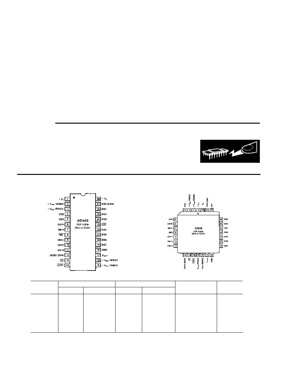
PIN DESIGNATIONS
ORDERING GUIDE
Integral Nonlinearity
Differential Nonlinearity
Temperature
Package
Model
1
+25 CTMIN–TMAX
Range
Option
2
AD569JN
±0.04%
±1 LSB
0
°C to +70°C
N-28
AD569JP
±0.04%
±1 LSB
0
°C to +70°C
P-28A
AD569KN
±0.024%
±1/2 LSB
±1 LSB
0
°C to +70°C
N-28
AD569KP
±0.024%
±1/2 LSB
±1 LSB
0
°C to +70°C
P-28A
AD569AD
±0.04%
±1 LSB
–25
°C to +85°C
D-28
AD569BD
±0.024%
±1/2 LSB
±1 LSB
–25
°C to +85°C
D-28
AD569SD
±0.04%
±1 LSB
–55
°C to +125°C
D-28
NOTES
1For details on grade and package offerings screened in accordance with MIL-STD-883, refer to the Analog Devices Military Products Databook
or current AD569/883B data sheet.
2D = Ceramic DIP; N = Plastic DIP; P = Plastic Leaded Chip Carrier.
WARNING!
ESD SENSITIVE DEVICE
相关PDF资料 |
PDF描述 |
|---|---|
| VE-B5T-MX-S | CONVERTER MOD DC/DC 6.5V 75W |
| VE-B5R-MX-S | CONVERTER MOD DC/DC 7.5V 75W |
| LTC1821-1AIGW#TRPBF | IC D/A CONV 16BIT PRECISE 36SSOP |
| LTC1821AIGW#TR | IC D/A CONV 16BIT PRECISE 36SSOP |
| VE-B5P-MX-S | CONVERTER MOD DC/DC 13.8V 75W |
相关代理商/技术参数 |
参数描述 |
|---|---|
| AD569JP-REEL | 功能描述:IC DAC 16BIT MONO NON-LIN 28PLCC RoHS:否 类别:集成电路 (IC) >> 数据采集 - 数模转换器 系列:- 产品培训模块:Lead (SnPb) Finish for COTS Obsolescence Mitigation Program 标准包装:1,000 系列:- 设置时间:1µs 位数:8 数据接口:串行 转换器数目:8 电压电源:双 ± 功率耗散(最大):941mW 工作温度:0°C ~ 70°C 安装类型:表面贴装 封装/外壳:24-SOIC(0.295",7.50mm 宽) 供应商设备封装:24-SOIC W 包装:带卷 (TR) 输出数目和类型:8 电压,单极 采样率(每秒):* |
| AD569JPZ | 功能描述:IC DAC 16BIT MONO NON-LIN 28PLCC RoHS:是 类别:集成电路 (IC) >> 数据采集 - 数模转换器 系列:- 产品培训模块:Lead (SnPb) Finish for COTS Obsolescence Mitigation Program 标准包装:50 系列:- 设置时间:4µs 位数:12 数据接口:串行 转换器数目:2 电压电源:单电源 功率耗散(最大):- 工作温度:-40°C ~ 85°C 安装类型:表面贴装 封装/外壳:8-TSSOP,8-MSOP(0.118",3.00mm 宽) 供应商设备封装:8-uMAX 包装:管件 输出数目和类型:2 电压,单极 采样率(每秒):* 产品目录页面:1398 (CN2011-ZH PDF) |
| AD569JPZ-REEL | 功能描述:IC DAC 16BIT MONO NON-LIN 28PLCC RoHS:是 类别:集成电路 (IC) >> 数据采集 - 数模转换器 系列:- 产品培训模块:Lead (SnPb) Finish for COTS Obsolescence Mitigation Program 标准包装:1,000 系列:- 设置时间:1µs 位数:8 数据接口:串行 转换器数目:8 电压电源:双 ± 功率耗散(最大):941mW 工作温度:0°C ~ 70°C 安装类型:表面贴装 封装/外壳:24-SOIC(0.295",7.50mm 宽) 供应商设备封装:24-SOIC W 包装:带卷 (TR) 输出数目和类型:8 电压,单极 采样率(每秒):* |
| AD569KN | 功能描述:IC DAC 16BIT MONO NON-LIN 28-DIP RoHS:否 类别:集成电路 (IC) >> 数据采集 - 数模转换器 系列:- 产品培训模块:Lead (SnPb) Finish for COTS Obsolescence Mitigation Program 标准包装:1,000 系列:- 设置时间:1µs 位数:8 数据接口:串行 转换器数目:8 电压电源:双 ± 功率耗散(最大):941mW 工作温度:0°C ~ 70°C 安装类型:表面贴装 封装/外壳:24-SOIC(0.295",7.50mm 宽) 供应商设备封装:24-SOIC W 包装:带卷 (TR) 输出数目和类型:8 电压,单极 采样率(每秒):* |
| AD569KNZ | 功能描述:IC DAC 16BIT MONOTONIC 28-DIP RoHS:是 类别:集成电路 (IC) >> 数据采集 - 数模转换器 系列:- 产品培训模块:Lead (SnPb) Finish for COTS Obsolescence Mitigation Program 标准包装:50 系列:- 设置时间:4µs 位数:12 数据接口:串行 转换器数目:2 电压电源:单电源 功率耗散(最大):- 工作温度:-40°C ~ 85°C 安装类型:表面贴装 封装/外壳:8-TSSOP,8-MSOP(0.118",3.00mm 宽) 供应商设备封装:8-uMAX 包装:管件 输出数目和类型:2 电压,单极 采样率(每秒):* 产品目录页面:1398 (CN2011-ZH PDF) |
发布紧急采购,3分钟左右您将得到回复。