参数资料
| 型号: | AD5732RBREZ |
| 厂商: | Analog Devices Inc |
| 文件页数: | 15/32页 |
| 文件大小: | 0K |
| 描述: | IC DAC DUAL 14BIT SERIAL 24TSSOP |
| 产品培训模块: | Data Converter Fundamentals DAC Architectures |
| 设计资源: | Software Configurable 14-Bit Dual-Channel Unipolar/Bipolar Voltage Output Using AD5732R (CN0090) |
| 标准包装: | 62 |
| 设置时间: | 10µs |
| 位数: | 14 |
| 数据接口: | 串行 |
| 转换器数目: | 2 |
| 电压电源: | 模拟和数字,双 ± |
| 功率耗散(最大): | 190mW |
| 工作温度: | -40°C ~ 85°C |
| 安装类型: | 表面贴装 |
| 封装/外壳: | 24-TSSOP(0.173",4.40mm)裸露焊盘 |
| 供应商设备封装: | 24-TSSOP 裸露焊盘 |
| 包装: | 管件 |
| 输出数目和类型: | 2 电压,单极;2 电压,双极 |
| 采样率(每秒): | 1.07M |
| 产品目录页面: | 784 (CN2011-ZH PDF) |
第1页第2页第3页第4页第5页第6页第7页第8页第9页第10页第11页第12页第13页第14页当前第15页第16页第17页第18页第19页第20页第21页第22页第23页第24页第25页第26页第27页第28页第29页第30页第31页第32页
AD5722R/AD5732R/AD5752R
Rev. D | Page 22 of 32
LOAD DAC (LDAC)
CONFIGURING THE AD5722R/AD5732R/AD5752R
When the power supplies are applied to the AD5722R/AD5732R/
AD5752R, the power-on reset circuit ensures that all registers
default to 0. This places all channels and the internal reference
in power-down mode. The DVCC should be brought high before
any of the interface lines are powered. If this is not done the first
write to the device may be ignored. The first communication to
the AD5722R/AD5732R/AD5752R should be to set the required
output range on all channels (the default range is the 5 V unipolar
range) by writing to the output range select register. The user
should then write to the power control register to power on the
required channels and the internal reference, if required.
After data has been transferred into the input register of the
DACs, there are two ways to update the DAC registers and DAC
outputs. Depending on the status of both SYNC and LDAC, one
of two update modes is selected: individual DAC updating or
simultaneous updating of all DACs.
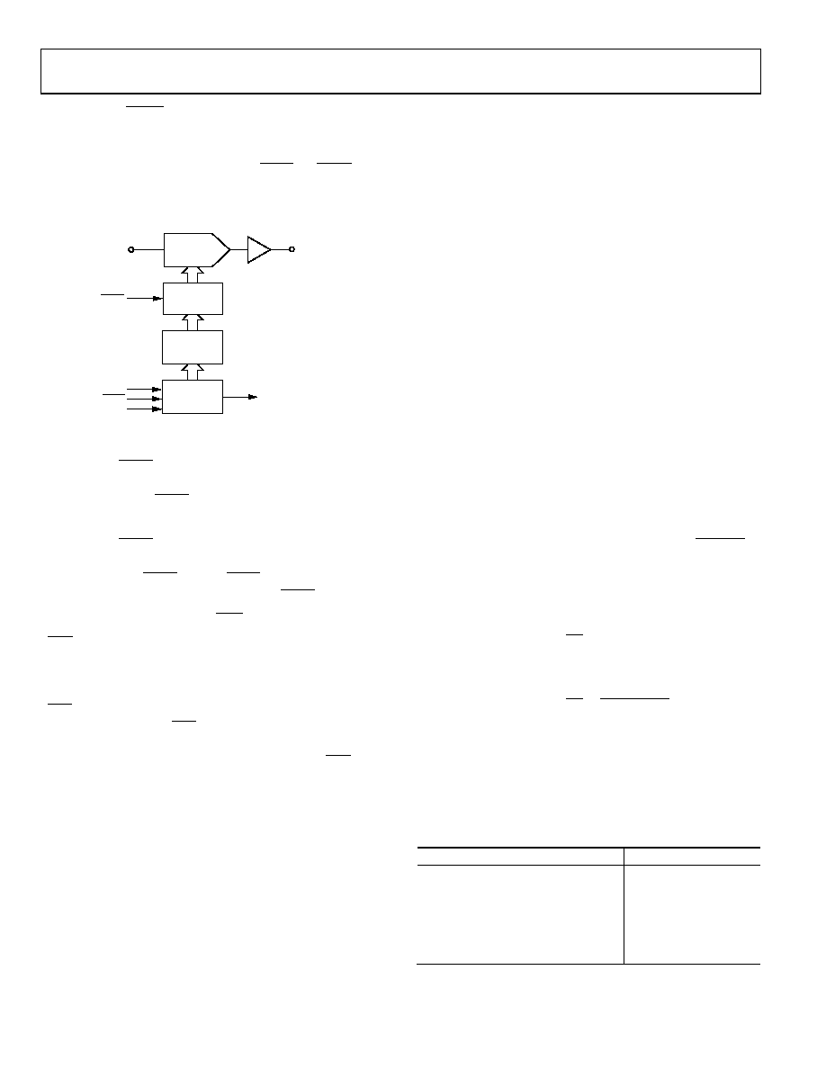
SYNC
SCLK
VOUTx
DAC
REGISTER
INTERFACE
LOGIC
OUTPUT
AMPLIFIER
LDAC
SDO
SDIN
REFIN
INPUT
REGISTER
12-/14-/16-BIT
DAC
06
46
6-
0
09
If an external reference source is being used, the internal
reference must remain in power-down mode. To program an
output value on a channel, that channel must first be powered
up; any writes to a channel while it is in power-down mode are
ignored. The AD5722R/AD5732R/AD5752R operate with a
wide power supply range. It is important that the power supply
applied to the parts provides adequate headroom to support the
chosen output ranges.
Figure 47. Simplified Diagram of Input Loading Circuitry for One DAC
Individual DAC Updating
TRANSFER FUNCTION
In this mode, LDAC is held low while data is being clocked into
the input shift register. The addressed DAC output is updated
on the rising edge of SYNC.
to output voltage for the AD5752R, AD5732R, and AD5722R,
respectively, for all output voltage ranges. For unipolar output
ranges, the data coding is straight binary. For bipolar output
ranges, the data coding is user selectable via the BIN/2sCOMP
pin and can be either offset binary or twos complement.
Simultaneous Updating of All DACs
In this mode, LDAC is held high while data is being clocked
into the input shift register. All DAC outputs are asynchronously
updated by taking LDAC low after SYNC has been taken high.
The update now occurs on the falling edge of LDAC.
For a unipolar output range, the output voltage expression is
given by
ASYNCHRONOUS CLEAR (CLR)
×
=
N
REFIN
OUT
D
Gain
V
2
CLR is an active low clear that allows the outputs to be cleared
to either zero-scale code or midscale code. The clear code value
is user selectable via the CLR select bit of the control register
(see the
section). It is necessary to maintain
CLR low for a minimum amount of time to complete the operation
(see
). When the
CLR signal is returned high, the output
remains at the cleared value until a new value is programmed. The
outputs cannot be updated with a new value while the CLR pin
is low. A clear operation can also be performed via the clear
command in the control register.
For a bipolar output range, the output voltage expression is given by
2
REFIN
N
REFIN
OUT
V
Gain
D
Gain
V
×
×
=
where:
D
is the decimal equivalent of the code loaded to the DAC.
N
is the bit resolution of the DAC.
VREFIN
is the reference voltage applied at the REFIN pin.
Gain
is an internal gain whose value depends on the output
range selected by the user, as shown in Table 7.
Table 7.
Output Range (V)
Gain Value
+5
2
+10
4
+10.8
4.32
±5
4
±10
8
±10.8
8.64
相关PDF资料 |
PDF描述 |
|---|---|
| GTC00R-22-19S | CONN RCPT 14POS WALL MNT W/SCKT |
| MS27473T18B96SA | CONN PLUG 9POS STRAIGHT W/SCKT |
| AD558JNZ | IC DAC 8BIT V-OUT 16-DIP |
| MS3450W28-21SZ | CONN RCPT 37POS WALL MNT W/SCKT |
| M83723/95R1808N | CONN PLUG 8POS STRAIGHT W/SCKT |
相关代理商/技术参数 |
参数描述 |
|---|---|
| AD5732RBREZ-REEL7 | 功能描述:IC DAC DUAL 14BIT SERIAL 24TSSOP RoHS:是 类别:集成电路 (IC) >> 数据采集 - 数模转换器 系列:- 标准包装:47 系列:- 设置时间:2µs 位数:14 数据接口:并联 转换器数目:1 电压电源:单电源 功率耗散(最大):55µW 工作温度:-40°C ~ 85°C 安装类型:表面贴装 封装/外壳:28-SSOP(0.209",5.30mm 宽) 供应商设备封装:28-SSOP 包装:管件 输出数目和类型:1 电流,单极;1 电流,双极 采样率(每秒):* |
| AD5734 | 制造商:AD 制造商全称:Analog Devices 功能描述:Complete, Quad, 12-/14-/16-Bit, Serial Input, Unipolar/Bipolar Voltage Output DACs |
| AD5734AREZ | 功能描述:IC DAC 14BIT DSP/SRL 24TSSOP RoHS:是 类别:集成电路 (IC) >> 数据采集 - 数模转换器 系列:- 标准包装:1 系列:- 设置时间:4.5µs 位数:12 数据接口:串行,SPI? 转换器数目:1 电压电源:单电源 功率耗散(最大):- 工作温度:-40°C ~ 125°C 安装类型:表面贴装 封装/外壳:8-SOIC(0.154",3.90mm 宽) 供应商设备封装:8-SOICN 包装:剪切带 (CT) 输出数目和类型:1 电压,单极;1 电压,双极 采样率(每秒):* 其它名称:MCP4921T-E/SNCTMCP4921T-E/SNRCTMCP4921T-E/SNRCT-ND |
| AD5734AREZ-REEL7 | 功能描述:IC DAC 14BIT DSP/SRL 24TSSOP RoHS:是 类别:集成电路 (IC) >> 数据采集 - 数模转换器 系列:- 标准包装:47 系列:- 设置时间:2µs 位数:14 数据接口:并联 转换器数目:1 电压电源:单电源 功率耗散(最大):55µW 工作温度:-40°C ~ 85°C 安装类型:表面贴装 封装/外壳:28-SSOP(0.209",5.30mm 宽) 供应商设备封装:28-SSOP 包装:管件 输出数目和类型:1 电流,单极;1 电流,双极 采样率(每秒):* |
| AD5734R | 制造商:AD 制造商全称:Analog Devices 功能描述:Complete, Quad, 12-/14-/16-Bit, Serial Input, Unipolar/Bipolar Voltage Output DACs |
发布紧急采购,3分钟左右您将得到回复。