参数资料
| 型号: | AD5732RBREZ |
| 厂商: | Analog Devices Inc |
| 文件页数: | 2/32页 |
| 文件大小: | 0K |
| 描述: | IC DAC DUAL 14BIT SERIAL 24TSSOP |
| 产品培训模块: | Data Converter Fundamentals DAC Architectures |
| 设计资源: | Software Configurable 14-Bit Dual-Channel Unipolar/Bipolar Voltage Output Using AD5732R (CN0090) |
| 标准包装: | 62 |
| 设置时间: | 10µs |
| 位数: | 14 |
| 数据接口: | 串行 |
| 转换器数目: | 2 |
| 电压电源: | 模拟和数字,双 ± |
| 功率耗散(最大): | 190mW |
| 工作温度: | -40°C ~ 85°C |
| 安装类型: | 表面贴装 |
| 封装/外壳: | 24-TSSOP(0.173",4.40mm)裸露焊盘 |
| 供应商设备封装: | 24-TSSOP 裸露焊盘 |
| 包装: | 管件 |
| 输出数目和类型: | 2 电压,单极;2 电压,双极 |
| 采样率(每秒): | 1.07M |
| 产品目录页面: | 784 (CN2011-ZH PDF) |
第1页当前第2页第3页第4页第5页第6页第7页第8页第9页第10页第11页第12页第13页第14页第15页第16页第17页第18页第19页第20页第21页第22页第23页第24页第25页第26页第27页第28页第29页第30页第31页第32页
AD5722R/AD5732R/AD5752R
Rev. D | Page 10 of 32
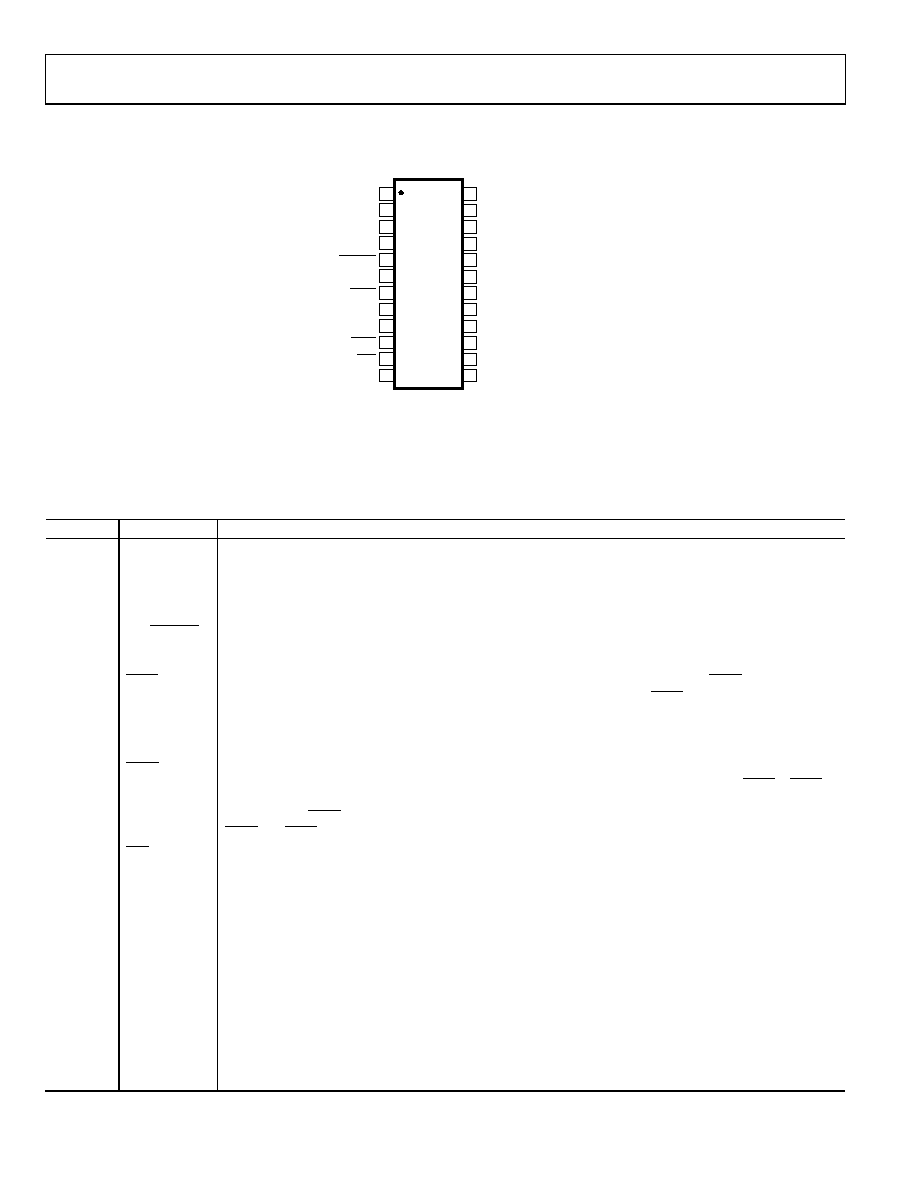
PIN CONFIGURATION AND FUNCTION DESCRIPTIONS
24
23
22
21
20
19
18
17
16
15
14
13
1
2
3
4
5
6
7
8
9
10
11
12
AD5722R/
AD5732R/
AD5752R
CLR
LDAC
AVSS
NC
VOUTA
NC
SYNC
NC
BIN/2sCOMP
GND
SDO
REFIN/REFOUT
SIG_GND
SCLK
SDIN
NC
NOTES
1. NC = NO CONNECT
2. IT IS RECOMMENDED THAT THE EXPOSED PAD BE
THERMALLY CONNECTED TO A COPPER PLANE
FOR ENHANCED THERMAL PERFORMANCE.
AVDD
VOUTB
NC
SIG_GND
DAC_GND
DVCC
NC
TOP VIEW
(Not to Scale)
06
46
6-
0
5
Figure 5. Pin Configuration
Table 6. Pin Function Descriptions
Pin No.
Mnemonic
Description
1
AVSS
Negative Analog Supply. Voltage ranges from 4.5 V to 16.5 V. This pin can be connected to 0 V if output
ranges are unipolar.
2, 4, 6, 12,
13, 22
NC
Do not connect to these pins.
3
VOUTA
Analog Output Voltage of DAC A. The output amplifier is capable of directly driving a 2 kΩ, 4000 pF load.
5
BIN/2sCOMP
Determines the DAC coding for a bipolar output range. This pin should be hardwired to either DVCC or GND.
When hardwired to DVCC, input coding is offset binary. When hardwired to GND, input coding is twos
complement. (For unipolar output ranges, coding is always straight binary.)
7
SYNC
Active Low Input. This is the frame synchronization signal for the serial interface. While SYNC is low, data is
transferred on the falling edge of SCLK. Data is latched on the rising edge of SYNC.
8
SCLK
Serial Clock Input. Data is clocked into the shift register on the falling edge of SCLK. This operates at clock
speeds up to 30 MHz.
9
SDIN
Serial Data Input. Data must be valid on the falling edge of SCLK.
10
LDAC
Load DAC, Logic Input. This is used to update the DAC registers and, consequently, the analog output. When
this pin is tied permanently low, the addressed DAC register is updated on the rising edge of SYNC. If LDAC is
held high during the write cycle, the DAC input register is updated, but the output update is held off until the
falling edge of LDAC. In this mode, all analog outputs can be updated simultaneously on the falling edge of
LDAC. The LDAC pin should not be left unconnected.
11
CLR
Active Low Input. Asserting this pin sets the DAC registers to zero-scale code or midscale code (user selectable).
14
DVCC
Digital Supply. Voltage ranges from 2.7 V to 5.5 V.
15
GND
Ground Reference.
16
SDO
Serial Data Output. Used to clock data from the serial register in daisy-chain or readback mode. Data is
clocked out on the rising edge of SCLK and is valid on the falling edge of SCLK.
17
REFIN/REFOUT
External Reference Voltage Input and Internal Reference Voltage Output. Reference input range is 2 V to 3 V.
REFIN = 2.5 V for specified performance. REFOUT = 2.5 V ± 2 mV.
18, 19
DAC_GND
Ground Reference for the Four Digital-to-Analog Converters.
20, 21
SIG_GND
Ground Reference for the Four Output Amplifiers.
23
VOUTB
Analog Output Voltage of DAC B. The output amplifier is capable of directly driving a 2 kΩ, 4000 pF load.
24
AVDD
Positive Analog Supply. Voltage ranges from 4.5 V to 16.5 V.
Exposed
Paddle
This exposed paddle should be connected to the potential of the AVSS pin, or alternatively, it can be left electrically
unconnected. It is recommended that the paddle be thermally connected to a copper plane for enhanced thermal
performance.
相关PDF资料 |
PDF描述 |
|---|---|
| GTC00R-22-19S | CONN RCPT 14POS WALL MNT W/SCKT |
| MS27473T18B96SA | CONN PLUG 9POS STRAIGHT W/SCKT |
| AD558JNZ | IC DAC 8BIT V-OUT 16-DIP |
| MS3450W28-21SZ | CONN RCPT 37POS WALL MNT W/SCKT |
| M83723/95R1808N | CONN PLUG 8POS STRAIGHT W/SCKT |
相关代理商/技术参数 |
参数描述 |
|---|---|
| AD5732RBREZ-REEL7 | 功能描述:IC DAC DUAL 14BIT SERIAL 24TSSOP RoHS:是 类别:集成电路 (IC) >> 数据采集 - 数模转换器 系列:- 标准包装:47 系列:- 设置时间:2µs 位数:14 数据接口:并联 转换器数目:1 电压电源:单电源 功率耗散(最大):55µW 工作温度:-40°C ~ 85°C 安装类型:表面贴装 封装/外壳:28-SSOP(0.209",5.30mm 宽) 供应商设备封装:28-SSOP 包装:管件 输出数目和类型:1 电流,单极;1 电流,双极 采样率(每秒):* |
| AD5734 | 制造商:AD 制造商全称:Analog Devices 功能描述:Complete, Quad, 12-/14-/16-Bit, Serial Input, Unipolar/Bipolar Voltage Output DACs |
| AD5734AREZ | 功能描述:IC DAC 14BIT DSP/SRL 24TSSOP RoHS:是 类别:集成电路 (IC) >> 数据采集 - 数模转换器 系列:- 标准包装:1 系列:- 设置时间:4.5µs 位数:12 数据接口:串行,SPI? 转换器数目:1 电压电源:单电源 功率耗散(最大):- 工作温度:-40°C ~ 125°C 安装类型:表面贴装 封装/外壳:8-SOIC(0.154",3.90mm 宽) 供应商设备封装:8-SOICN 包装:剪切带 (CT) 输出数目和类型:1 电压,单极;1 电压,双极 采样率(每秒):* 其它名称:MCP4921T-E/SNCTMCP4921T-E/SNRCTMCP4921T-E/SNRCT-ND |
| AD5734AREZ-REEL7 | 功能描述:IC DAC 14BIT DSP/SRL 24TSSOP RoHS:是 类别:集成电路 (IC) >> 数据采集 - 数模转换器 系列:- 标准包装:47 系列:- 设置时间:2µs 位数:14 数据接口:并联 转换器数目:1 电压电源:单电源 功率耗散(最大):55µW 工作温度:-40°C ~ 85°C 安装类型:表面贴装 封装/外壳:28-SSOP(0.209",5.30mm 宽) 供应商设备封装:28-SSOP 包装:管件 输出数目和类型:1 电流,单极;1 电流,双极 采样率(每秒):* |
| AD5734R | 制造商:AD 制造商全称:Analog Devices 功能描述:Complete, Quad, 12-/14-/16-Bit, Serial Input, Unipolar/Bipolar Voltage Output DACs |
发布紧急采购,3分钟左右您将得到回复。