- 您现在的位置:买卖IC网 > PDF目录8633 > AD5734AREZ-REEL7 (Analog Devices Inc)IC DAC 14BIT DSP/SRL 24TSSOP PDF资料下载
参数资料
| 型号: | AD5734AREZ-REEL7 |
| 厂商: | Analog Devices Inc |
| 文件页数: | 17/32页 |
| 文件大小: | 0K |
| 描述: | IC DAC 14BIT DSP/SRL 24TSSOP |
| 产品培训模块: | Data Converter Fundamentals DAC Architectures |
| 设计资源: | Software Configurable 14-Bit Quad-Channel Unipolar/Bipolar Voltage Output Using AD5734 (CN0087) |
| 标准包装: | 1,000 |
| 设置时间: | 10µs |
| 位数: | 14 |
| 数据接口: | DSP,MICROWIRE?,QSPI?,串行,SPI? |
| 转换器数目: | 4 |
| 电压电源: | 模拟和数字,双 ± |
| 功率耗散(最大): | 310mW |
| 工作温度: | -40°C ~ 85°C |
| 安装类型: | 表面贴装 |
| 封装/外壳: | 24-TSSOP(0.173",4.40mm)裸露焊盘 |
| 供应商设备封装: | 24-TSSOP 裸露焊盘 |
| 包装: | 带卷 (TR) |
| 输出数目和类型: | 4 电压,单极;4 电压,双极 |
| 采样率(每秒): | 100k |
第1页第2页第3页第4页第5页第6页第7页第8页第9页第10页第11页第12页第13页第14页第15页第16页当前第17页第18页第19页第20页第21页第22页第23页第24页第25页第26页第27页第28页第29页第30页第31页第32页
AD5724/AD5734/AD5754
Rev. D | Page 24 of 32
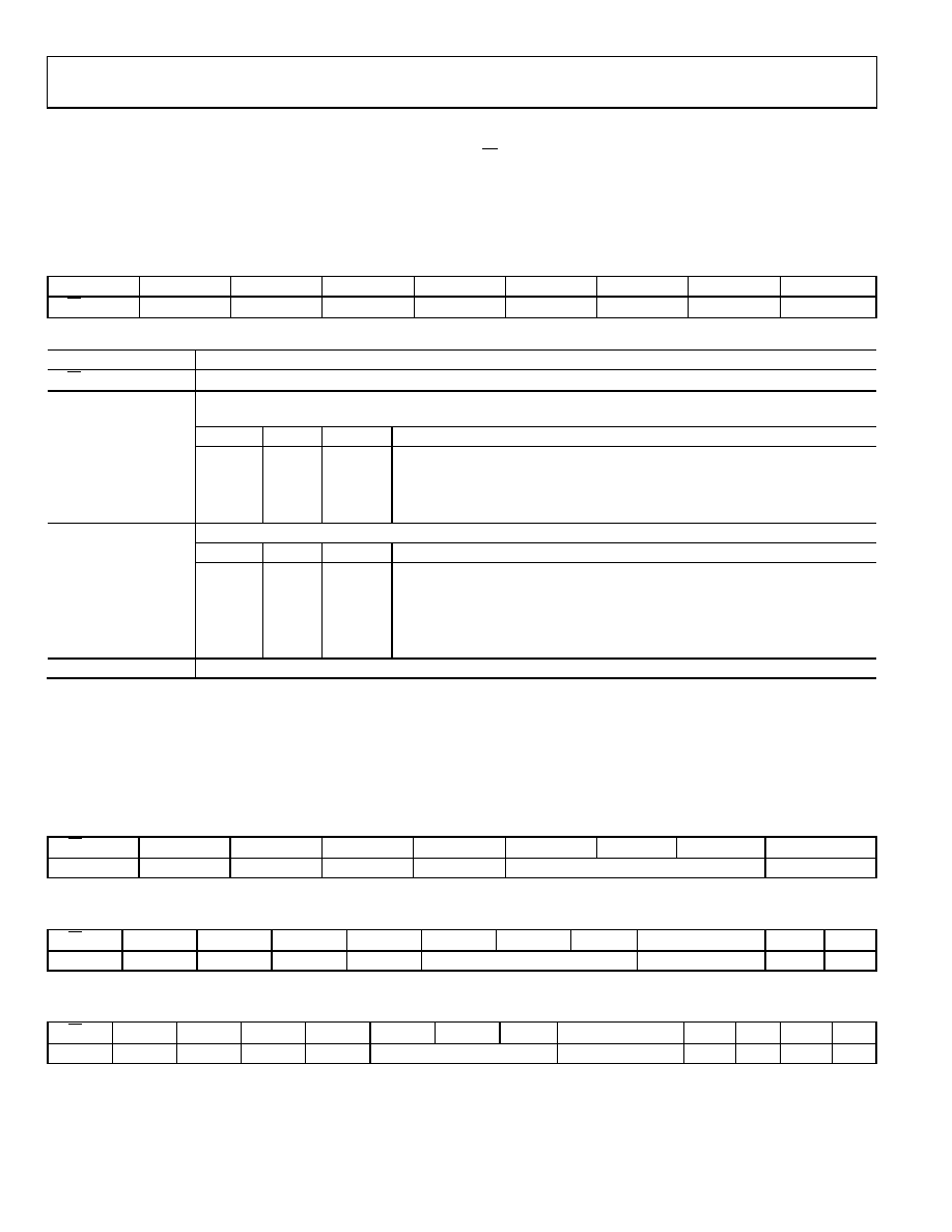
INPUT SHIFT REGISTER
The input shift register is 24 bits wide and consists of a read/write bit (R/W), a reserved bit (zero) that must always be set to 0, three
register select bits (REG0, REG1, REG2), three DAC address bits (A2, A1, A0), and 16 data bits (data). The register data is clocked in MSB
first on the SDIN pin.
shows the register format and
describes the function of each bit in the register. All registers are
read/write registers.
Table 16. Input Register Format
MSB
LSB
DB23
DB22
DB21
DB20
DB19
DB18
DB17
DB16
DB15 to DB0
R/W
Zero
REG2
REG1
REG0
A2
A1
A0
Data
Table 17. Input Register Bit Functions
Bit Mnemonic
Description
R/W
Indicates a read from or a write to the addressed register.
REG2, REG1, REG0
Used in association with the address bits to determine if a write operation is to the DAC register, the output range
select register, the power control register, or the control register.
REG2
REG1
REG0
Function
0
DAC register
0
1
Output range select register
0
1
0
Power control register
0
1
Control register
A2, A1, A0
These DAC address bits are used to decode the DAC channels.
A2
A1
A0
Channel Address
0
DAC A
0
1
DAC B
0
1
0
DAC C
0
1
DAC D
1
0
All four DACs
DB15 to DB0
Data bits.
DAC REGISTER
The DAC register is addressed by setting the three REG bits to 000. The DAC address bits select the DAC channel where the data transfer
is to take place (see Table 17). The data bits are in positions DB15 to DB0 for the AD5754 (see Table 18), DB15 to DB2 for the AD5734
Table 18. Programming the AD5754 DAC Register
MSB
LSB
R/W
Zero
REG2
REG1
REG0
A2
A1
A0
DB15 to DB0
0
DAC address
16-bit DAC data
Table 19. Programming the AD5734 DAC Register
MSB
LSB
R/W
Zero
REG2
REG1
REG0
A2
A1
A0
DB15 to DB2
DB1
DB0
0
DAC address
14-bit DAC data
X
Table 20. Programming the AD5724 DAC Register
MSB
LSB
R/W
Zero
REG2
REG1
REG0
A2
A1
A0
DB15 to DB4
DB3
DB2
DB1
DB0
0
DAC address
12-bit DAC data
X
相关PDF资料 |
PDF描述 |
|---|---|
| VE-J30-MW-S | CONVERTER MOD DC/DC 5V 100W |
| AD7545AKP-REEL | IC DAC 12BIT W/BUFF MULT 20-PLCC |
| VE-22X-MW-B1 | CONVERTER MOD DC/DC 5.2V 100W |
| VE-B3X-MX-S | CONVERTER MOD DC/DC 5.2V 75W |
| VE-B3W-MX-S | CONVERTER MOD DC/DC 5.5V 75W |
相关代理商/技术参数 |
参数描述 |
|---|---|
| AD5734R | 制造商:AD 制造商全称:Analog Devices 功能描述:Complete, Quad, 12-/14-/16-Bit, Serial Input, Unipolar/Bipolar Voltage Output DACs |
| AD5734RBREZ | 功能描述:IC DAC 14BIT DSP/SRL 24TSSOP RoHS:是 类别:集成电路 (IC) >> 数据采集 - 数模转换器 系列:- 产品培训模块:Lead (SnPb) Finish for COTS Obsolescence Mitigation Program 标准包装:50 系列:- 设置时间:4µs 位数:12 数据接口:串行 转换器数目:2 电压电源:单电源 功率耗散(最大):- 工作温度:-40°C ~ 85°C 安装类型:表面贴装 封装/外壳:8-TSSOP,8-MSOP(0.118",3.00mm 宽) 供应商设备封装:8-uMAX 包装:管件 输出数目和类型:2 电压,单极 采样率(每秒):* 产品目录页面:1398 (CN2011-ZH PDF) |
| AD5734RBREZ-REEL7 | 功能描述:IC DAC 14BIT DSP/SRL 24TSSOP RoHS:是 类别:集成电路 (IC) >> 数据采集 - 数模转换器 系列:- 产品培训模块:Data Converter Fundamentals DAC Architectures 标准包装:750 系列:- 设置时间:7µs 位数:16 数据接口:并联 转换器数目:1 电压电源:双 ± 功率耗散(最大):100mW 工作温度:0°C ~ 70°C 安装类型:表面贴装 封装/外壳:28-LCC(J 形引线) 供应商设备封装:28-PLCC(11.51x11.51) 包装:带卷 (TR) 输出数目和类型:1 电压,单极;1 电压,双极 采样率(每秒):143k |
| AD5735 | 制造商:AD 制造商全称:Analog Devices 功能描述:Quad Channel, 16-Bit, Serial Input, 4-20mA & Voltage Output DAC, Dynamic Power Control |
| AD5735_12 | 制造商:AD 制造商全称:Analog Devices 功能描述:Quad-Channel, 12-Bit, Serial Input, 4 mA to 20 mA |
发布紧急采购,3分钟左右您将得到回复。