- 您现在的位置:买卖IC网 > PDF目录8633 > AD5734AREZ-REEL7 (Analog Devices Inc)IC DAC 14BIT DSP/SRL 24TSSOP PDF资料下载
参数资料
| 型号: | AD5734AREZ-REEL7 |
| 厂商: | Analog Devices Inc |
| 文件页数: | 21/32页 |
| 文件大小: | 0K |
| 描述: | IC DAC 14BIT DSP/SRL 24TSSOP |
| 产品培训模块: | Data Converter Fundamentals DAC Architectures |
| 设计资源: | Software Configurable 14-Bit Quad-Channel Unipolar/Bipolar Voltage Output Using AD5734 (CN0087) |
| 标准包装: | 1,000 |
| 设置时间: | 10µs |
| 位数: | 14 |
| 数据接口: | DSP,MICROWIRE?,QSPI?,串行,SPI? |
| 转换器数目: | 4 |
| 电压电源: | 模拟和数字,双 ± |
| 功率耗散(最大): | 310mW |
| 工作温度: | -40°C ~ 85°C |
| 安装类型: | 表面贴装 |
| 封装/外壳: | 24-TSSOP(0.173",4.40mm)裸露焊盘 |
| 供应商设备封装: | 24-TSSOP 裸露焊盘 |
| 包装: | 带卷 (TR) |
| 输出数目和类型: | 4 电压,单极;4 电压,双极 |
| 采样率(每秒): | 100k |
第1页第2页第3页第4页第5页第6页第7页第8页第9页第10页第11页第12页第13页第14页第15页第16页第17页第18页第19页第20页当前第21页第22页第23页第24页第25页第26页第27页第28页第29页第30页第31页第32页
AD5724/AD5734/AD5754
Rev. D | Page 28 of 32
APPLICATIONS INFORMATION
+5 V/±5 V OPERATION
When operating from a single +5 V supply or a dual ±5 V supply,
an output range of +5 V or ±5 V is not achievable because
sufficient headroom for the output amplifier is not available.
In this situation, a reduced reference voltage can be used. For
example, a 2 V reference voltage produces an output range of
+4 V or ±4 V, and the 1 V of headroom is more than enough for
full operation. A standard value voltage reference of 2.048 V can
be used to produce output ranges of +4.096 V and ±4.096 V.
LAYOUT GUIDELINES
In any circuit where accuracy is important, careful consideration
of the power supply and ground return layout helps to ensure
the rated performance. The printed circuit board on which the
AD5724/AD5734/AD5754 are mounted should be designed so
that the analog and digital sections are separated and confined
to certain areas of the board. If the AD5724/AD5734/AD5754
are in a system where multiple devices require an AGND-to-
DGND connection, the connection should be made at one
point only. The star ground point should be established as close
as possible to the device.
The AD5724/AD5734/AD5754 should have ample supply bypass-
ing of a 10 μF capacitor in parallel with a 0.1 μF capacitor on
each supply located as close to the package as possible, ideally
right up against the device. The 10 μF capacitor is the tantalum
bead type. The 0.1 μF capacitor should have low effective series
resistance (ESR) and low effective series inductance (ESI), such
as the common ceramic types, which provide a low impedance
path to ground at high frequencies to handle transient currents
due to internal logic switching.
The power supply lines of the AD5724/AD5734/AD5754 should
use as large a trace as possible to provide low impedance paths
and reduce the effects of glitches on the power supply line. Fast
switching signals, such as a data clock, should be shielded with
digital ground to avoid radiating noise to other parts of the
board, and they should never be run near the reference inputs.
A ground line routed between the SDIN and SCLK lines helps
reduce crosstalk between them (this is not required on a multilayer
board that has a separate ground plane, but separating the lines
does help). It is essential to minimize noise on the REFIN line
because any unwanted signals will couple through to the DAC
outputs.
Avoid crossover of digital and analog signals. Traces on opposite
sides of the board should run at right angles to each other. This
reduces the effects of feedthrough on the board. A microstrip
technique is by far the best method, but it is not always possible
with a double-sided board. In this technique, the component
side of the board is dedicated to a ground plane, and signal
traces are placed on the solder side.
GALVANICALLY ISOLATED INTERFACE
In many process control applications, it is necessary to provide
an isolation barrier between the controller and the unit being
controlled to protect and isolate the controlling circuitry from
any hazardous common-mode voltages that may occur. The
i
Coupler family of products from Analog Devices, Inc., provides
voltage isolation in excess of 2.5 kV. The serial loading structure
of the AD5724/AD5734/AD5754 makes them ideal for isolated
interfaces because the number of interface lines is kept to a
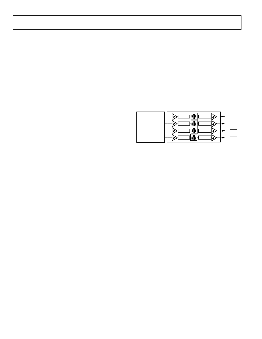
minimum. Figure 43 shows a 4-channel isolated interface to the
AD5724/AD5734/AD5754 using an ADuM1400. For further
information, visit http://www.analog.com/icouplers.
ENCODE
DECODE
ENCODE
DECODE
ENCODE
DECODE
VIA
VIB
VIC
VID
VOA
VOB
VOC
VOD
ENCODE
DECODE
ADuM1400*
MICROCONTROLLER
SERIAL CLOCK OUT
SERIAL DATA OUT
SYNC OUT
CONTROL OUT
TO SCLK
TO SDIN
TO SYNC
TO LDAC
*ADDITIONAL PINS OMITTED FOR CLARITY.
06
46
8-
01
1
Figure 43. Isolated Interface
VOLTAGE REFERENCE SELECTION
To achieve optimum performance from the AD5724/AD5734/
AD5754 over their full operating temperature range, a precision
voltage reference must be used. Thought should be given to the
selection of a precision voltage reference. The voltage applied to
the reference inputs are used to provide a buffered positive and
negative reference for the DAC cores. Therefore, any error in
the voltage reference is reflected in the outputs of the device.
There are four possible sources of error to consider when
choosing a voltage reference for high accuracy applications:
initial accuracy, temperature coefficient of the output voltage,
long-term drift, and output voltage noise.
Initial accuracy error on the output voltage of an external
reference can lead to a full-scale error in the DAC.
Therefore, to minimize these errors, a reference with low
initial accuracy error specification is preferred. Choosing a
reference with an output trim adjustment, such as the
ADR421, allows a system designer to trim out system
errors by setting the reference voltage to a voltage other
than the nominal. The trim adjustment can also be used to
trim out temperature-induced errors.
The temperature coefficient of a reference output voltage
affects INL, DNL, and TUE. A reference with a tight
temperature coefficient specification should be chosen to
reduce the dependence of the DAC output voltage on
ambient conditions.
Long-term drift is a measure of how much the reference
output voltage drifts over time. A reference with a tight
long-term drift specification ensures that the overall
solution remains relatively stable over its entire lifetime.
相关PDF资料 |
PDF描述 |
|---|---|
| VE-J30-MW-S | CONVERTER MOD DC/DC 5V 100W |
| AD7545AKP-REEL | IC DAC 12BIT W/BUFF MULT 20-PLCC |
| VE-22X-MW-B1 | CONVERTER MOD DC/DC 5.2V 100W |
| VE-B3X-MX-S | CONVERTER MOD DC/DC 5.2V 75W |
| VE-B3W-MX-S | CONVERTER MOD DC/DC 5.5V 75W |
相关代理商/技术参数 |
参数描述 |
|---|---|
| AD5734R | 制造商:AD 制造商全称:Analog Devices 功能描述:Complete, Quad, 12-/14-/16-Bit, Serial Input, Unipolar/Bipolar Voltage Output DACs |
| AD5734RBREZ | 功能描述:IC DAC 14BIT DSP/SRL 24TSSOP RoHS:是 类别:集成电路 (IC) >> 数据采集 - 数模转换器 系列:- 产品培训模块:Lead (SnPb) Finish for COTS Obsolescence Mitigation Program 标准包装:50 系列:- 设置时间:4µs 位数:12 数据接口:串行 转换器数目:2 电压电源:单电源 功率耗散(最大):- 工作温度:-40°C ~ 85°C 安装类型:表面贴装 封装/外壳:8-TSSOP,8-MSOP(0.118",3.00mm 宽) 供应商设备封装:8-uMAX 包装:管件 输出数目和类型:2 电压,单极 采样率(每秒):* 产品目录页面:1398 (CN2011-ZH PDF) |
| AD5734RBREZ-REEL7 | 功能描述:IC DAC 14BIT DSP/SRL 24TSSOP RoHS:是 类别:集成电路 (IC) >> 数据采集 - 数模转换器 系列:- 产品培训模块:Data Converter Fundamentals DAC Architectures 标准包装:750 系列:- 设置时间:7µs 位数:16 数据接口:并联 转换器数目:1 电压电源:双 ± 功率耗散(最大):100mW 工作温度:0°C ~ 70°C 安装类型:表面贴装 封装/外壳:28-LCC(J 形引线) 供应商设备封装:28-PLCC(11.51x11.51) 包装:带卷 (TR) 输出数目和类型:1 电压,单极;1 电压,双极 采样率(每秒):143k |
| AD5735 | 制造商:AD 制造商全称:Analog Devices 功能描述:Quad Channel, 16-Bit, Serial Input, 4-20mA & Voltage Output DAC, Dynamic Power Control |
| AD5735_12 | 制造商:AD 制造商全称:Analog Devices 功能描述:Quad-Channel, 12-Bit, Serial Input, 4 mA to 20 mA |
发布紧急采购,3分钟左右您将得到回复。