参数资料
| 型号: | AD5750-2BCPZ |
| 厂商: | Analog Devices Inc |
| 文件页数: | 3/36页 |
| 文件大小: | 0K |
| 描述: | IC CURR/VOLT OUT DRIVER 32LFCSP |
| 标准包装: | 1 |
| 放大器类型: | 仪表 |
| 电路数: | 1 |
| 转换速率: | 2 V/µs |
| 电流 - 电源: | 5.2mA |
| 电流 - 输出 / 通道: | 24mA |
| 电压 - 电源,单路/双路(±): | ±12 V ~ 24 V |
| 工作温度: | -40°C ~ 105°C |
| 安装类型: | 表面贴装 |
| 封装/外壳: | 32-VFQFN 裸露焊盘,CSP |
| 供应商设备封装: | 32-LFCSP(5x5) |
| 包装: | 托盘 |
第1页第2页当前第3页第4页第5页第6页第7页第8页第9页第10页第11页第12页第13页第14页第15页第16页第17页第18页第19页第20页第21页第22页第23页第24页第25页第26页第27页第28页第29页第30页第31页第32页第33页第34页第35页第36页
Data Sheet
AD5750/AD5750-1/AD5750-2
Rev. E | Page 11 of 36
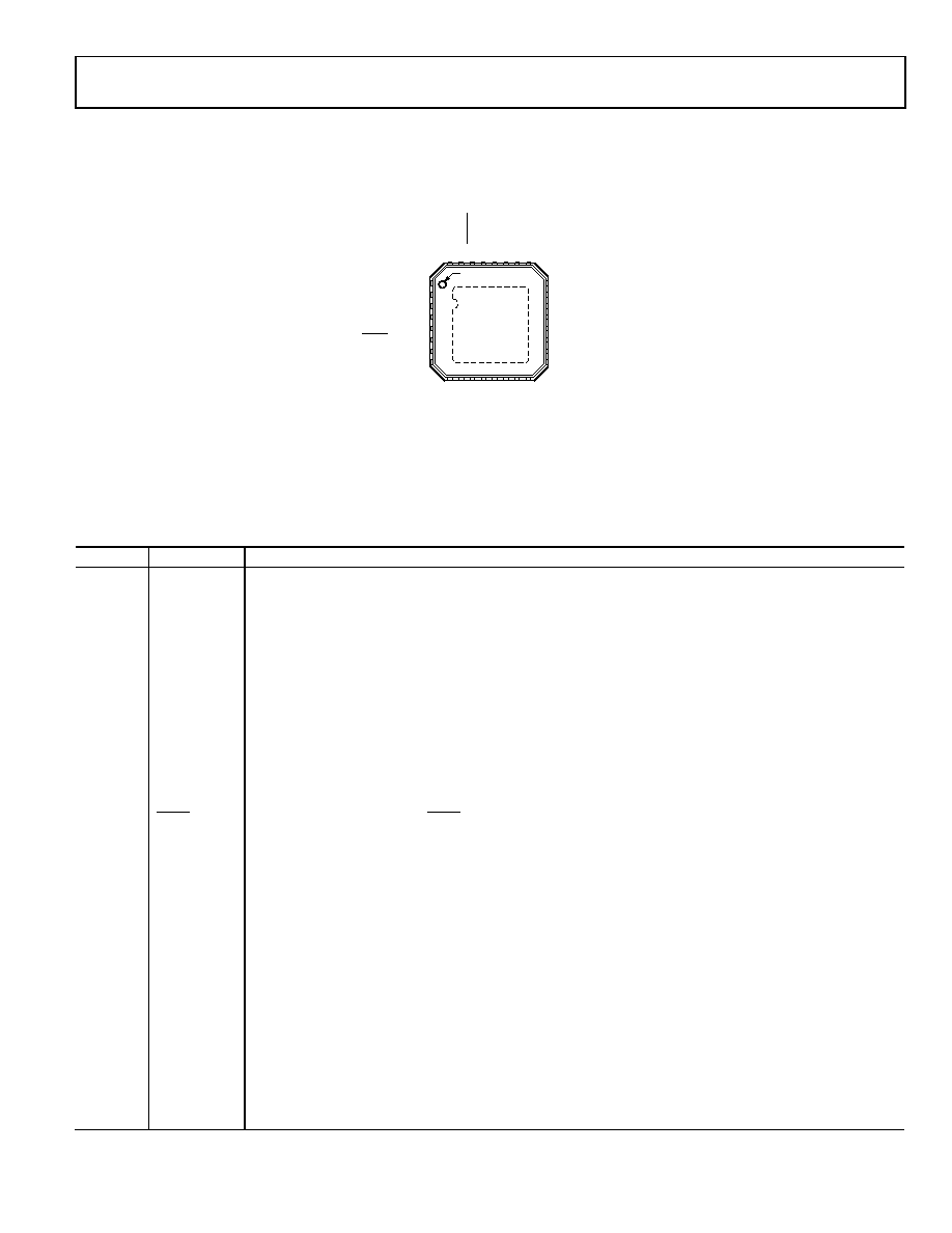
PIN CONFIGURATION AND FUNCTION DESCRIPTIONS
Figure 4. Pin Configuration
Table 5. Pin Function Descriptions
Pin No.
Mnemonic
Description
1
SDO/VFAULT
Serial Data Output (SDO). In software mode, this pin is used to clock data from the input shift register in
readback mode. Data is clocked out on the rising edge of SCLK and is valid on the falling edge of SCLK. This pin
is a CMOS output.
Short-Circuit Fault Alert (VFAULT). In hardware mode, this pin acts as a short-circuit fault alert pin and is
asserted low when a short-circuit error is detected. This pin is an open-drain output and must be connected to
a pull-up resistor.
2
CLRSEL
In hardware or software mode, this pin selects the clear value, either zero-scale or midscale code. In software
mode, this pin is implemented as a logic OR with the internal CLRSEL bit.
3
CLEAR
Active High Input. Asserting this pin sets the output current/voltage to zero-scale code or midscale code of the
range selected (user selectable). CLEAR is a logic OR with the internal clear bit.
In software mode, during power-up, the CLEAR pin level determines the power-on condition of the voltage
channel, which can be active 0 V or tristate. See the Asynchronous Clear (CLEAR) section for more details.
4
DVCC
Digital Power Supply.
5
GND
Ground Connection.
6
SYNC/RSET
Positive Edge Sensitive Latch (SYNC). In software mode, a rising edge parallel loads the input shift register data
Resistor Select (RSET). In hardware mode, this pin selects whether the internal or the external current sense resistor is
used. If RSET = 0, the external sense resistor is chosen, and if RSET = 1, the internal sense resistor is chosen.
7
SCLK/OUTEN
Serial Clock Input (SCLK). In software mode, data is clocked into the input shift register on the falling edge of
SCLK. This pin operates at clock speeds up to 50 MHz.
Output Enable (OUTEN). In hardware mode, this pin acts as an output enable pin.
8
SDIN/R0
Serial Data Input (SDIN). In software mode, data must be valid on the falling edge of SCLK.
Range Decode Bit (R0). In hardware mode, this pin, in conjunction with R1, R2, and R3, selects the output
current/voltage range setting on the part.
9
AD2/R1
Device Addressing Bit (AD2). In software mode, this pin, in conjunction with AD1 and AD0, allows up to eight
devices to be addressed on one bus.
Range Decode Bit (R1). In hardware mode, this pin, in conjunction with R0, R2, and R3, selects the output
current/voltage range setting on the part.
10
AD1/R2
Device Addressing Bit (AD1). In software mode, this pin, in conjunction with AD2 and AD0, allows up to eight
devices to be addressed on one bus.
Range Decode Bit (R2). In hardware mode, this pin, in conjunction with R0, R1, and R3, selects the output
current/voltage range setting on the part.
PIN 1
INDICATOR
TOP VIEW
(Not to Scale)
AD5750/
AD5750-1/
AD5750-2
1
SDO/VFAULT
2
CLRSEL
3
CLEAR
4
DVCC
5
GND
6
SYNC/RSET
7
SCLK/OUTEN
8
SDIN/R0
24 VSENSE+
23 VOUT
22 VSENSE–
21 AVSS
20 COMP1
19 COMP2
18 IOUT
17 AVDD
9
A
D
2
/R
1
0
A
D
1
/R
2
1
A
D
0
/R
3
1
2
R
E
X
T
2
1
3
R
E
X
T
1
4
V
R
E
F
1
5
V
IN
1
6
G
N
D
3
2
N
C
/I
F
A
U
L
T
3
1
F
A
U
L
T
/T
E
M
P
3
0
R
E
S
E
T
2
9
H
W
S
E
L
E
C
T
2
8
N
C
2
7
N
C
2
6
N
C
2
5
N
C
NOTES
1. NC = NO CONNECT.
2. THE EXPOSED PADDLE IS TIED TO AVSS.
0
726
8-
0
05
相关PDF资料 |
PDF描述 |
|---|---|
| GTCA38-501M-R10-FS2 | GAS TUBE 8MM 500V 20% 10KA |
| ADA4637-1ARZ | IC OPAMP JFET 79.9MHZ LN 8SOIC |
| HTSW-101-08-G-S | CONN HEADER 1POS .100" T/H GOLD |
| LT1491IS#PBF | IC OP-AMP R-R IN/OUT QUAD 14SOIC |
| ADA4897-2ARMZ | IC OPAMP RR 230MHZ LP 10MSOP |
相关代理商/技术参数 |
参数描述 |
|---|---|
| AD5750-2BCPZ-RL7 | 功能描述:IC CURR/VOLT OUT DRVR 32LFCSP RoHS:是 类别:集成电路 (IC) >> Linear - Amplifiers - Instrumentation 系列:- 标准包装:73 系列:Over-The-Top® 放大器类型:通用 电路数:4 输出类型:满摆幅 转换速率:0.07 V/µs 增益带宽积:200kHz -3db带宽:- 电流 - 输入偏压:1nA 电压 - 输入偏移:285µV 电流 - 电源:50µA 电流 - 输出 / 通道:25mA 电压 - 电源,单路/双路(±):2 V ~ 44 V,±1 V ~ 22 V 工作温度:-40°C ~ 85°C 安装类型:表面贴装 封装/外壳:16-WFDFN 裸露焊盘 供应商设备封装:16-DFN-EP(5x3) 包装:管件 |
| AD5750ACPZ | 功能描述:IC CURR/VOLT OUT DVR 32LFCSP RoHS:是 类别:集成电路 (IC) >> Linear - Amplifiers - Instrumentation 系列:- 标准包装:1 系列:- 放大器类型:通用 电路数:4 输出类型:满摆幅 转换速率:0.028 V/µs 增益带宽积:105kHz -3db带宽:- 电流 - 输入偏压:3nA 电压 - 输入偏移:100µV 电流 - 电源:3.3µA 电流 - 输出 / 通道:12mA 电压 - 电源,单路/双路(±):2.7 V ~ 12 V,±1.35 V ~ 6 V 工作温度:-40°C ~ 85°C 安装类型:表面贴装 封装/外壳:14-TSSOP(0.173",4.40mm 宽) 供应商设备封装:14-TSSOP 包装:剪切带 (CT) 其它名称:OP481GRUZ-REELCT |
| AD5750ACPZ-REEL | 功能描述:IC CURR/VOLT OUT DVR 32LFCSP RoHS:是 类别:集成电路 (IC) >> Linear - Amplifiers - Instrumentation 系列:- 标准包装:100 系列:- 放大器类型:通用 电路数:1 输出类型:- 转换速率:0.2 V/µs 增益带宽积:- -3db带宽:- 电流 - 输入偏压:100pA 电压 - 输入偏移:30µV 电流 - 电源:380µA 电流 - 输出 / 通道:- 电压 - 电源,单路/双路(±):±2 V ~ 18 V 工作温度:0°C ~ 70°C 安装类型:表面贴装 封装/外壳:8-SOIC(0.154",3.90mm 宽) 供应商设备封装:8-SO 包装:管件 |
| AD5750ACPZ-REEL7 | 功能描述:IC CURR/VOLT OUT DVR 32LFCSP RoHS:是 类别:集成电路 (IC) >> Linear - Amplifiers - Instrumentation 系列:- 标准包装:100 系列:- 放大器类型:通用 电路数:1 输出类型:- 转换速率:0.2 V/µs 增益带宽积:- -3db带宽:- 电流 - 输入偏压:100pA 电压 - 输入偏移:30µV 电流 - 电源:380µA 电流 - 输出 / 通道:- 电压 - 电源,单路/双路(±):±2 V ~ 18 V 工作温度:0°C ~ 70°C 安装类型:表面贴装 封装/外壳:8-SOIC(0.154",3.90mm 宽) 供应商设备封装:8-SO 包装:管件 |
| AD5750BCPZ | 功能描述:IC CURR/VOLT OUT DVR 32LFCSP RoHS:是 类别:集成电路 (IC) >> Linear - Amplifiers - Instrumentation 系列:- 标准包装:150 系列:- 放大器类型:音频 电路数:2 输出类型:- 转换速率:5 V/µs 增益带宽积:12MHz -3db带宽:- 电流 - 输入偏压:100nA 电压 - 输入偏移:500µV 电流 - 电源:6mA 电流 - 输出 / 通道:50mA 电压 - 电源,单路/双路(±):4 V ~ 32 V,±2 V ~ 16 V 工作温度:-40°C ~ 85°C 安装类型:表面贴装 封装/外壳:8-TSSOP(0.173",4.40mm 宽) 供应商设备封装:8-TSSOP 包装:管件 |
发布紧急采购,3分钟左右您将得到回复。