参数资料
| 型号: | AD5750BCPZ-REEL |
| 厂商: | Analog Devices Inc |
| 文件页数: | 18/36页 |
| 文件大小: | 0K |
| 描述: | IC CURR/VOLT OUT DVR 32LFCSP |
| 标准包装: | 5,000 |
| 放大器类型: | 仪表 |
| 电路数: | 1 |
| 转换速率: | 2 V/µs |
| 电流 - 电源: | 5.2mA |
| 电流 - 输出 / 通道: | 24mA |
| 电压 - 电源,单路/双路(±): | ±10.8 V ~ 26.4 V |
| 工作温度: | -40°C ~ 105°C |
| 安装类型: | 表面贴装 |
| 封装/外壳: | 32-VFQFN 裸露焊盘,CSP |
| 供应商设备封装: | 32-LFCSP-VQ(5x5) |
| 包装: | 带卷 (TR) |
第1页第2页第3页第4页第5页第6页第7页第8页第9页第10页第11页第12页第13页第14页第15页第16页第17页当前第18页第19页第20页第21页第22页第23页第24页第25页第26页第27页第28页第29页第30页第31页第32页第33页第34页第35页第36页
AD5750/AD5750-1
Rev. C | Page 25 of 36
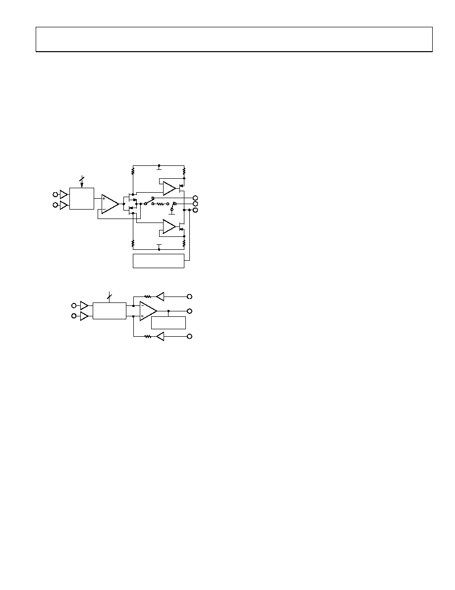
CURRENT OUTPUT ARCHITECTURE
The voltage input from the analog input VIN pin (0 V to 4.096 V
for AD5750; 0 V to 2.5 V for the AD5750-1) is either converted
to a current (see Figure 53), which is then mirrored to the
supply rail so that the application simply sees a current source
output with respect to an internal reference voltage, or it is
buffered and scaled to output a software-selectable unipolar or
bipolar voltage range (see Figure 54). The reference is used to
provide internal offsets for range and gain scaling. The
selectable output range is programmable through the digital
interface.
IOUT
RANGE
SCALING
REXT1
IOUT
RSET
Vx
VSS
VDD
R1
R4
R2
R3
REXT2
IOUT
OPEN FAULT
VIN
VREF
RANGE DECODE
FROM INTERFACE
07
268
-0
47
Figure 53. Current Output Configuration
VOUT RANGE
SCALING
VSENSE+
VOUT
VSENSE–
VOUT
SHORT FAULT
RANGE DECODE
FROM INTERFACE
VIN
(0V TO 4.096V)
VREF
072
68-
0
48
Figure 54. Voltage Output
DRIVING INDUCTIVE LOADS
When driving inductive or poorly defined loads, connect a 0.01 μF
capacitor between IOUT and GND. This ensures stability with
loads beyond 50 mH. There is no maximum capacitance limit.
The capacitive component of the load may cause slower settling.
Voltage Output Amplifier
The voltage output amplifier is capable of generating both
unipolar and bipolar output voltages. It is capable of driving a
load of 1 kΩ in parallel with 1.2 μF (with an external compensa-
tion capacitor on the COMP1 and COMP2 pins). The source
and sink capabilities of the output amplifier can be seen in
Figure 16. The slew rate is 2 V/μs.
Internal to the device, there is a 2.5 MΩ resistor connected
between the VOUT and VSENSE+ pins and similarly between
the VSENSE pin and the internal device ground. Should a
fault condition occur, these resistors act to protect the AD5750/
AD5750-1 by ensuring the amplifier loop is closed so that the
part does not enter into an open-loop condition.
The VSENSE pin can work in a common-mode range of ±3 V
with respect to the remote load ground point.
The current and voltage are output on separate pins and cannot
be output simultaneously. This allows the user to tie both the
current and voltage output pins together and configure the end
system as a single-channel output.
Driving Large Capacitive Loads
The voltage output amplifier is capable of driving capacitive loads
of up to 1 μF with the addition of a nonpolarized compensation
capacitor between the COMP1 and COMP2 pins.
Without the compensation capacitor, up to 20 nF capacitive loads
can be driven. Care should be taken to choose an appropriate
value for the CCOMP capacitor. This capacitor, while allowing the
AD5750/AD5750-1 to drive higher capacitive loads and reduce
overshoot, increases the settling time of the part and therefore
affects the bandwidth of the system. Considered values of this
capacitor should be in the range 100 pF to 4 nF, depending on
the trade-off required between settling time, overshoot, and
bandwidth.
POWER-ON STATE OF AD5750/AD5750-1
On power-up, the AD5750/AD5750-1 sense whether hardware
or software mode is loaded and set the power-up conditions
accordingly.
In software SPI mode, the power-up state of the output is
dependent on the state of the CLEAR pin. If the CLEAR pin is
pulled high, then the part powers up, driving an active 0 V on
the output. If the CLEAR pin is pulled low, then the part powers
up with the voltage output channel in tristate mode. In both
cases, the current output channel powers up in the tristate
condition (0 mA). This allows the voltage and current outputs
to be connected together if desired.
To put the part into normal operation, the user must set the
OUTEN bit in the control register to enable the output and, in
the same write, set the output range configuration using the R3
to R0 range bits. If the CLEAR pin is still high (active) during
this write, the part automatically clears to its normal clear state
as defined by the programmed range and by the CLRSEL pin or
the CLRSEL bit (see the Asynchronous Clear (CLEAR) section
for more details). The CLEAR pin must be taken low to operate
the part in normal mode.
The CLEAR pin is typically driven directly from a microcontroller.
In cases where the power supply for the AD5750/AD5750-1
supply may be independent of the microcontroller power supply,
the user can connect a weak pull-up resistor to DVCC or a pull-
down resistor to ground to ensure that the correct power-up
condition is achieved independent of the microcontroller. A
10 kΩ pull-up/pull-down resistor on the CLEAR pin should be
sufficient for most applications.
If hardware mode is selected, the part powers up to the condi-
tions defined by the R3 to R0 range bits and the status of the
OUTEN or CLEAR pin. It is recommended to keep the output
disabled when powering up the part in hardware mode.
相关PDF资料 |
PDF描述 |
|---|---|
| RNCP0603FTD274R | RES 274 OHM 1% 0603 SMD |
| TSW-137-26-G-D | CONN HEADER 74POS .100" DL GOLD |
| 77313-119-04LF | BERGSTIK |
| ISL28325FUZ-T7A | IC OP AMP 1.2MHZ DUAL LP 8MSOP |
| Y17455K00000T9R | RES 5.0K OHM .25W .01% Z-FOIL SM |
相关代理商/技术参数 |
参数描述 |
|---|---|
| AD5750BCPZ-REEL7 | 功能描述:IC CURR/VOLT OUT DVR 32LFCSP RoHS:是 类别:集成电路 (IC) >> Linear - Amplifiers - Instrumentation 系列:- 标准包装:73 系列:Over-The-Top® 放大器类型:通用 电路数:4 输出类型:满摆幅 转换速率:0.07 V/µs 增益带宽积:200kHz -3db带宽:- 电流 - 输入偏压:1nA 电压 - 输入偏移:285µV 电流 - 电源:50µA 电流 - 输出 / 通道:25mA 电压 - 电源,单路/双路(±):2 V ~ 44 V,±1 V ~ 22 V 工作温度:-40°C ~ 85°C 安装类型:表面贴装 封装/外壳:16-WFDFN 裸露焊盘 供应商设备封装:16-DFN-EP(5x3) 包装:管件 |
| AD5751 | 制造商:AD 制造商全称:Analog Devices 功能描述:Industrial Current/Voltage Output Driver |
| AD5751ACPZ | 功能描述:IC CURR/VOLT OUT DVR 32LFCSP RoHS:是 类别:集成电路 (IC) >> Linear - Amplifiers - Instrumentation 系列:- 标准包装:2,500 系列:Excalibur™ 放大器类型:J-FET 电路数:1 输出类型:- 转换速率:45 V/µs 增益带宽积:10MHz -3db带宽:- 电流 - 输入偏压:20pA 电压 - 输入偏移:490µV 电流 - 电源:1.7mA 电流 - 输出 / 通道:48mA 电压 - 电源,单路/双路(±):4.5 V ~ 38 V,±2.25 V ~ 19 V 工作温度:-40°C ~ 85°C 安装类型:表面贴装 封装/外壳:8-SOIC(0.154",3.90mm 宽) 供应商设备封装:8-SOIC 包装:带卷 (TR) |
| AD5751ACPZ | 制造商:Analog Devices 功能描述:IC CURRENT/VOLTAGE O/P DRIVER LFCSP-32 |
| AD5751ACPZ-REEL7 | 功能描述:IC I/V OUTPUT DRIVER 60V 32LFCSP RoHS:是 类别:集成电路 (IC) >> Linear - Amplifiers - Instrumentation 系列:- 标准包装:50 系列:- 放大器类型:J-FET 电路数:2 输出类型:- 转换速率:3.5 V/µs 增益带宽积:1MHz -3db带宽:- 电流 - 输入偏压:30pA 电压 - 输入偏移:2000µV 电流 - 电源:200µA 电流 - 输出 / 通道:- 电压 - 电源,单路/双路(±):7 V ~ 36 V,±3.5 V ~ 18 V 工作温度:0°C ~ 70°C 安装类型:通孔 封装/外壳:8-DIP(0.300",7.62mm) 供应商设备封装:8-PDIP 包装:管件 |
发布紧急采购,3分钟左右您将得到回复。