- 您现在的位置:买卖IC网 > PDF目录8582 > AD5765BSUZ-REEL7 (Analog Devices Inc)IC DAC 16BIT 5V QUAD 32-TQFP PDF资料下载
参数资料
| 型号: | AD5765BSUZ-REEL7 |
| 厂商: | Analog Devices Inc |
| 文件页数: | 18/28页 |
| 文件大小: | 0K |
| 描述: | IC DAC 16BIT 5V QUAD 32-TQFP |
| 产品培训模块: | Data Converter Fundamentals DAC Architectures |
| 产品变化通告: | AD5763/65 Metal Layer Edit Change 08/Sept/2009 |
| 设计资源: | High Accuracy, Bipolar Voltage Output Digital-to-Analog Conversion Using AD5765 (CN0073) |
| 标准包装: | 500 |
| 设置时间: | 8µs |
| 位数: | 16 |
| 数据接口: | 串行 |
| 转换器数目: | 4 |
| 电压电源: | 双 ± |
| 功率耗散(最大): | 76mW |
| 工作温度: | -40°C ~ 105°C |
| 安装类型: | 表面贴装 |
| 封装/外壳: | 32-TQFP |
| 供应商设备封装: | 32-TQFP(7x7) |
| 包装: | 带卷 (TR) |
| 输出数目和类型: | 4 电压,双极 |
| 采样率(每秒): | * |
第1页第2页第3页第4页第5页第6页第7页第8页第9页第10页第11页第12页第13页第14页第15页第16页第17页当前第18页第19页第20页第21页第22页第23页第24页第25页第26页第27页第28页
Data Sheet
AD5765
Rev. C | Page 25 of 28
APPLICATIONS INFORMATION
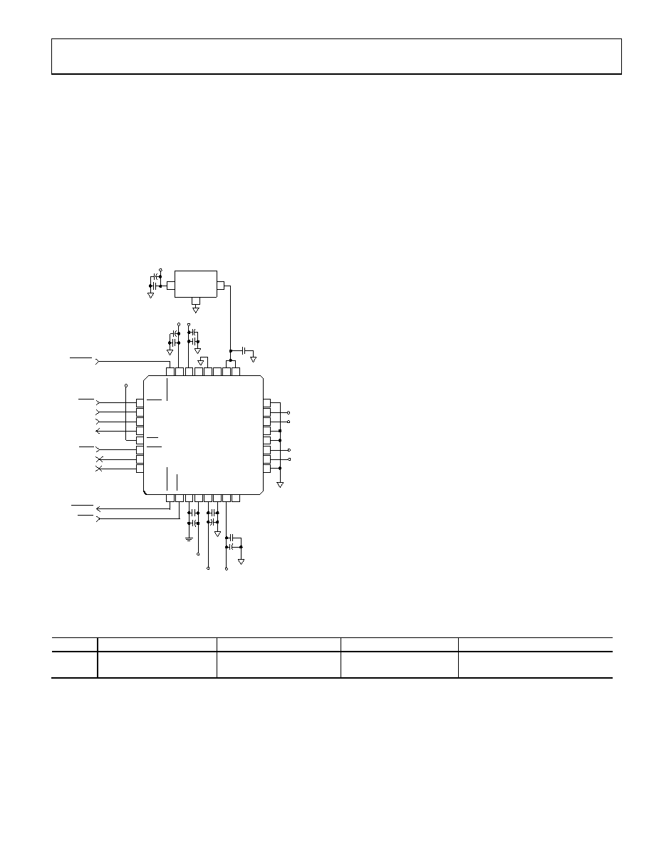
TYPICAL OPERATING CIRCUIT
Figure 29 shows the typical operating circuit for the AD5765.
The only external components needed for this precision 16-bit
DAC are a reference voltage source, decoupling capacitors on
the supply pins and reference inputs, and an optional short-
circuit current setting resistor. Because the device incorporates
reference buffers, it eliminates the need for an external bipolar
reference and associated buffers. This leads to an overall savings
in both cost and board space.
to 5 V. In Figure 29, AGNDx is connected to REFGND.
1
2
3
4
5
6
7
8
23
22
21
18
19
20
24
17
9
10 11
12
13 14 15
16
32 31 30
29 28 27 26
25
AD5765
SYNC
SCLK
SDIN
SDO
D0
LDAC
CLR
D1
VOUTA
VOUTB
AGNDB
VOUTD
VOUTC
AGNDC
AGNDA
AGNDD
RS
T
O
UT
R
S
TIN
DG
ND
DV
CC
AV
DD
P
G
ND
AV
SS
IS
CC
BI
N/
2sCO
M
P
AV
DD
AV
SS
T
EMP
RE
F
G
ND
NC
RE
F
CD
RE
F
AB
SYNC
SCLK
SDIN
SDO
LDAC
D0
D1
RSTOUT
RSTIN
BIN/2sCOMP
+5V
–5V
NC = NO CONNECT
+5V –5V
VOUTA
VOUTB
VOUTC
VOUTD
100nF
100n
F
100n
F
10F
100nF
10F
10
F
10F
ADR420
4
GND
2
6
VOUT
VIN
+5V
100nF
10F
07249-
035
Figure 29. Typical Operating Circuit
PRECISION VOLTAGE REFERENCE SELECTION
To achieve the optimum performance from the AD5765 over its
full operating temperature range, a precision voltage reference
must be used. Thought should be given to the selection of a
precision voltage reference. The AD5765 has two reference
inputs, REFAB and REFCD. The voltages applied to the
reference inputs are used to provide a buffered positive and
negative reference for the DAC cores. Therefore, any error in
the voltage reference is reflected in the outputs of the device.
There are four possible sources of error to consider when
choosing a voltage reference for high accuracy applications:
initial accuracy, temperature coefficient of the output voltage,
long-term drift, and output voltage noise.
Initial accuracy error on the output voltage of an external refer-
ence may lead to a full-scale error in the DAC. Therefore, to
minimize these errors, a reference with low initial accuracy
error specification is preferred. Choosing a reference with an
output trim adjustment, such as the ADR430, allows a system
designer to trim system errors out by setting the reference
voltage to a voltage other than the nominal. The trim adjust-
ment can also be used at temperature to trim out any error.
Long-term drift is a measure of how much the reference output
voltage drifts over time. A reference with a tight long-term drift
specification ensures that the overall solution remains relatively
stable over its entire lifetime.
The temperature coefficient of a reference output voltage affects
INL, DNL, and TUE. A reference with a tight temperature
coefficient specification should be chosen to reduce the
dependence of the DAC output voltage on ambient conditions.
In high accuracy applications (which have a relatively low noise
budget), reference output voltage noise needs to be considered.
Choosing a reference with as low an output noise voltage as
practical for the system resolution required is important.
Precision voltage references such as the ADR420 (XFET design)
produce low output noise in the 0.1 Hz to 10 Hz region.
However, as the circuit bandwidth increases, filtering the output
of the reference may be required to minimize the output noise.
Table 21. Some Precision References Recommended for Use with the AD5765
Part No.
Initial Accuracy (mV Max)
Long-Term Drift (ppm Typ)
Temp Drift (ppm/°C Max)
0.1 Hz to 10 Hz Noise (V p-p Typ)
±1
40
3
3.5
±1
50
3
1.75
相关PDF资料 |
PDF描述 |
|---|---|
| VI-B61-MU | CONVERTER MOD DC/DC 12V 200W |
| LTC2754BCUKG-16#TRPBF | IC DAC 16BIT QUAD IOUT 52-QFN |
| VI-B4X-MU | CONVERTER MOD DC/DC 5.2V 200W |
| VI-21V-IV-F1 | CONVERTER MOD DC/DC 5.8V 150W |
| VI-B40-MU | CONVERTER MOD DC/DC 5V 200W |
相关代理商/技术参数 |
参数描述 |
|---|---|
| AD5765CSUZ | 功能描述:IC DAC 16BIT QUAD 5V 1LSB 32TQFP RoHS:是 类别:集成电路 (IC) >> 数据采集 - 数模转换器 系列:- 标准包装:1 系列:- 设置时间:4.5µs 位数:12 数据接口:串行,SPI? 转换器数目:1 电压电源:单电源 功率耗散(最大):- 工作温度:-40°C ~ 125°C 安装类型:表面贴装 封装/外壳:8-SOIC(0.154",3.90mm 宽) 供应商设备封装:8-SOICN 包装:剪切带 (CT) 输出数目和类型:1 电压,单极;1 电压,双极 采样率(每秒):* 其它名称:MCP4921T-E/SNCTMCP4921T-E/SNRCTMCP4921T-E/SNRCT-ND |
| AD5765CSUZ-REEL7 | 功能描述:IC DAC 16BIT 5V QUAD 32-TQFP RoHS:是 类别:集成电路 (IC) >> 数据采集 - 数模转换器 系列:- 产品培训模块:Data Converter Fundamentals DAC Architectures 标准包装:750 系列:- 设置时间:7µs 位数:16 数据接口:并联 转换器数目:1 电压电源:双 ± 功率耗散(最大):100mW 工作温度:0°C ~ 70°C 安装类型:表面贴装 封装/外壳:28-LCC(J 形引线) 供应商设备封装:28-PLCC(11.51x11.51) 包装:带卷 (TR) 输出数目和类型:1 电压,单极;1 电压,双极 采样率(每秒):143k |
| AD5766BCBZ-RL7 | 功能描述:16 CHANNEL 16 BIT BIPOLAR DAC 制造商:analog devices inc. 系列:- 零件状态:在售 位数:16 数模转换器数:16 建立时间:12μs 输出类型:Voltage - Unbuffered 差分输出:无 数据接口:SPI,DSP 参考类型:外部 电压 - 电源,模拟:2.97 V ~ 16 V 电压 - 电源,数字:- INL/DNL(LSB):±16,±1 架构:电阻串 DAC 工作温度:-40°C ~ 105°C 封装/外壳:49-UFBGA,WLCSP 供应商器件封装:49-WLCSP 标准包装:1 |
| AD5767BCBZ-RL7 | 功能描述:16 CHANNEL 12 BIT BIPOLAR DAC 制造商:analog devices inc. 系列:- 包装:剪切带(CT) 零件状态:在售 位数:12 数模转换器数:16 建立时间:12μs 输出类型:Voltage - Unbuffered 差分输出:无 数据接口:SPI,DSP 参考类型:外部 电压 - 电源,模拟:2.97 V ~ 16 V 电压 - 电源,数字:- INL/DNL(LSB):±1,±1 架构:电阻串 DAC 工作温度:-40°C ~ 105°C 封装/外壳:49-UFBGA,WLCSP 供应商器件封装:49-WLCSP 标准包装:1 |
| AD5767BCPZ-RL7 | 功能描述:16 CHANNEL 12 BIT BIPOLAR DAC 制造商:analog devices inc. 系列:- 包装:剪切带(CT) 零件状态:在售 位数:12 数模转换器数:16 建立时间:12μs 输出类型:Voltage - Unbuffered 差分输出:无 数据接口:SPI,DSP 参考类型:外部 电压 - 电源,模拟:2.97 V ~ 16 V 电压 - 电源,数字:- INL/DNL(LSB):±1,±1 架构:电阻串 DAC 工作温度:-40°C ~ 105°C 封装/外壳:40-WFQFN 裸露焊盘,CSP 供应商器件封装:40-LFCSP(6x6) 标准包装:1 |
发布紧急采购,3分钟左右您将得到回复。