- 您现在的位置:买卖IC网 > PDF目录11674 > AD598AD (Analog Devices Inc)IC LVDT SIGNAL COND 20-CDIP PDF资料下载
参数资料
| 型号: | AD598AD |
| 厂商: | Analog Devices Inc |
| 文件页数: | 13/16页 |
| 文件大小: | 0K |
| 描述: | IC LVDT SIGNAL COND 20-CDIP |
| 标准包装: | 1 |
| 类型: | 信号调节器 |
| 输入类型: | 电压 |
| 输出类型: | 电压 |
| 接口: | LVDT |
| 电流 - 电源: | 15mA |
| 安装类型: | 通孔 |
| 封装/外壳: | 20-CDIP(0.300",7.62mm) |
| 供应商设备封装: | 20-CDIP |
| 包装: | 管件 |
| 产品目录页面: | 790 (CN2011-ZH PDF) |
AD598
REV. A
–6–
DESIGN PROCEDURE
DUAL SUPPLY OPERATION
Figure 7 shows the connection method with dual
±15 volt power
supplies and a Schaevitz E100 LVDT. This design procedure
can be used to select component values for other LVDTs as
well. The procedure is outlined in Steps 1 through 10 as follows:
1. Determine the mechanical bandwidth required for LVDT
position measurement subsystem, fSUBSYSTEM. For this
example, assume fSUBSYSTEM = 250 Hz.
2. Select minimum LVDT excitation frequency, approximately
10
× f
SUBSYSTEM. Therefore, let excitation frequency = 2.5 kHz.
3. Select a suitable LVDT that will operate with an excitation
frequency of 2.5 kHz. The Schaevitz E100, for instance, will
operate over a range of 50 Hz to 10 kHz and is an eligible
candidate for this example.
4. Determine the sum of LVDT secondary voltages VA and VB.
Energize the LVDT at its typical drive level VPRI as shown in
the manufacturer’s data sheet (3 V rms for the E100). Set the
core displacement to its center position where VA = VB. Mea-
sure these values and compute their sum VA+VB. For the
E100, VA+VB = 2.70 V rms. This calculation will be used
later in determining AD598 output voltage.
5. Determine optimum LVDT excitation voltage, VEXC. With
the LVDT energized at its typical drive level VPRI, set the
core displacement to its mechanical full-scale position and
measure the output VSEC of whichever secondary produces
the largest signal. Compute LVDT voltage transformation
ratio, VTR.
VTR = VPRI/VSEC
For the E100, VSEC = 1.71 V rms for VPRI = 3 V rms.
VTR = 1.75.
The AD598 signal input, VSEC, should be in the range of
1 V rms to 3.5 V rms for maximum AD598 linearity and
minimum noise susceptibility. Select VSEC = 3 V rms. There-
fore, LVDT excitation voltage VEXC should be:
VEXC = VSEC
× VTR = 3 × 1.75 = 5.25 V rms
Check the power supply voltages by verifying that the peak
values of VA and VB are at least 2.5 volts less than the volt-
ages at +VS and –VS.
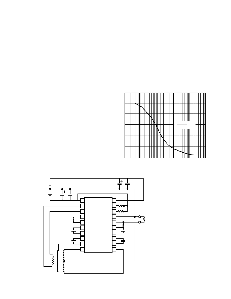
6. Referring to Figure 7, for VS =
±15 V, select the value of the
amplitude determining component R1 as shown by the curve
in Figure 8.
7. Select excitation frequency determining component C1.
C1 = 35
F Hz/f
EXCITATION
30
20
10
0
0.01
0.1
1
10
100
1000
R1 – k
Vrms
V
EXC
–
V
rms
Figure 8. Excitation Voltage VEXC vs. R1
EXC 1
EXC 2
LEV 1
LEV 2
FREQ 1
FREQ 2
B1 FILT
B2 FILT
OFFSET 1
OFFSET 2
SIG REF
SIG OUT
FEEDBACK
OUT FILT
A1 FILT
A2 FILT
R1
C1
C2
AD598
C3
R2
C4
LVDT
SCHAEVITZ E100
R3
R4
6.8
F
0.1
F
0.1
F
6.8
F
–15V
SIGNAL
REFERENCE
15V
+
–VS
R
L
VOUT
+VS
1
2
3
4
5
6
7
8
9
10
11
12
13
14
16
15
17
18
19
20
NOTE
FOR C1, C2, C3 AND C4 MYLAR
CAPACITORS ARE
RECOMMENDED. CERAMIC
CAPACITORS MAY BE
SUBSTITUTED. FOR R2, R3 AND
R4 USE STANDARD 1%
RESISTORS.
V
A
V
B
V
B
V
A
Figure 7. Interconnection Diagram for Dual Supply Operation
相关PDF资料 |
PDF描述 |
|---|---|
| AD2S90APZ | IC R/D CONV 12BIT 20-PLCC |
| 226990-3 | CONN JACK BNC RT/A 50OHM PCB AU |
| AD598JRZ | IC LVDT SGNL COND OSC/REF 20SOIC |
| 221185-2 | CONN PLUG BNC 75 OHM DUAL CRIMP |
| AD698APZ | IC LVDT SIGNAL COND 28-PLCC |
相关代理商/技术参数 |
参数描述 |
|---|---|
| AD598AD | 制造商:Analog Devices 功能描述:SEMICONDUCTORS LINEAR |
| AD598J | 制造商:AD 制造商全称:Analog Devices 功能描述:LVDT Signal Conditioner |
| AD598JR | 功能描述:IC LVDT SGNL COND OSC/REF 20SOIC RoHS:否 类别:集成电路 (IC) >> 接口 - 传感器和探测器接口 系列:- 其它有关文件:Automotive Product Guide 产品培训模块:Lead (SnPb) Finish for COTS Obsolescence Mitigation Program 标准包装:74 系列:- 类型:触控式传感器 输入类型:数字 输出类型:数字 接口:JTAG,串行 电流 - 电源:100µA 安装类型:表面贴装 封装/外壳:20-TSSOP(0.173",4.40mm 宽) 供应商设备封装:20-TSSOP 包装:管件 |
| AD598JRZ | 功能描述:IC LVDT SGNL COND OSC/REF 20SOIC RoHS:是 类别:集成电路 (IC) >> 接口 - 传感器和探测器接口 系列:- 其它有关文件:Automotive Product Guide 产品培训模块:Lead (SnPb) Finish for COTS Obsolescence Mitigation Program 标准包装:74 系列:- 类型:触控式传感器 输入类型:数字 输出类型:数字 接口:JTAG,串行 电流 - 电源:100µA 安装类型:表面贴装 封装/外壳:20-TSSOP(0.173",4.40mm 宽) 供应商设备封装:20-TSSOP 包装:管件 |
| AD598JRZ | 制造商:Analog Devices 功能描述:Signal Conditioner IC |
发布紧急采购,3分钟左右您将得到回复。