参数资料
| 型号: | AD600ARZ |
| 厂商: | Analog Devices Inc |
| 文件页数: | 11/33页 |
| 文件大小: | 0K |
| 描述: | IC AMP VGA DUAL LN 50MA 16SOIC |
| 标准包装: | 1 |
| 系列: | X-AMP® |
| 放大器类型: | 可变增益 |
| 电路数: | 2 |
| 转换速率: | 275 V/µs |
| -3db带宽: | 35MHz |
| 电流 - 输入偏压: | 350nA |
| 电流 - 电源: | 11mA |
| 电流 - 输出 / 通道: | 50mA |
| 电压 - 电源,单路/双路(±): | ±4.75 V ~ 5.25 V |
| 工作温度: | -40°C ~ 85°C |
| 安装类型: | 表面贴装 |
| 封装/外壳: | 16-SOIC(0.295",7.50mm 宽) |
| 供应商设备封装: | 16-SOIC W |
| 包装: | 管件 |
| 产品目录页面: | 774 (CN2011-ZH PDF) |
第1页第2页第3页第4页第5页第6页第7页第8页第9页第10页当前第11页第12页第13页第14页第15页第16页第17页第18页第19页第20页第21页第22页第23页第24页第25页第26页第27页第28页第29页第30页第31页第32页第33页
AD600/AD602
Rev. F | Page 18 of 32
FREQUENCY (MHz)
AG
C
O
UT
P
UT
CHANG
E
(
d
B
)
1
100
10
0.1
A simple half-wave detector is used based on Q1 and R2. The
average current into Capacitor C2 is the difference between the
current provided by the AD590 (300 μA at 300 K, 27°C) and the
collector current of Q1. In turn, the control voltage, VG, is the
time integral of this error current. When VG (thus the gain) is
stable, the rectified current in Q1 must, on average, balance
exactly the current in the AD590. If the output of A2 is too small
to do this, VG ramps up, causing the gain to increase until Q1
conducts sufficiently. The operation of this control system follows.
First, consider the particular case where R2 is zero and the
output voltage, VOUT, is a square wave at, for example, 100 kHz,
well above the corner frequency of the control loop. During the
time VOUT is negative, Q1 conducts. When VOUT is positive, it is
cut off. Because the average collector current is forced to be
300 μA and the square wave has a 50% duty-cycle, the current
when conducting must be 600 μA. With R2 omitted, the peak
value of VOUT would be just the VBE of Q1 at 600 μA (typically
about 700 mV) or 2 VBE p-p. This voltage, thus the amplitude at
which the output stabilizes, has a strong negative temperature
coefficient (TC), typically –1.7 mV/°C. While this may not be
troublesome in some applications, the correct value of R2
renders the output stable with temperature.
To understand this, first note that the current in the AD590 is
closely proportional to absolute temperature (PTAT). In fact,
this IC is intended for use as a thermometer. For the moment,
assume that the signal is a square wave. When Q1 is conducting,
VOUT is the sum of VBE and a voltage that is PTAT and that can
be chosen to have an equal but opposite TC of the base-to-
emitter voltage. This is actually nothing more than the band gap
voltage reference principle thinly disguised. When R2 is chosen
so that the sum of the voltage across it and the VBE of Q1 is close
to the band gap voltage of about 1.2 V, VOUT is stable over a wide
range of temperatures, provided that Q1 and the AD590 share the
same thermal environment.
Because the average emitter current is 600 μA during each half-
cycle of the square wave, a resistor of 833 Ω would add a PTAT
voltage of 500 mV at 300 K, increasing by 1.66 mV/°C. In
practice, the optimum value of R2 depends on the transistor
used and, to a lesser extent, on the waveform for which the
temperature stability is to be optimized; for the devices shown
and sine wave signals, the recommended value is 806 Ω. This
resistor also serves to lower the peak current in Q1, and the
200 Hz LP filter it forms with C2 helps to minimize distortion
due to ripple in VG. Note that the output amplitude under sine
wave conditions is higher than for a square wave because the
average value of the current for an ideal rectifier would be
0.637 times as large, causing the output amplitude to be 1.88 V
(= 1.2/0.637), or 1.33 V rms. In practice, the somewhat nonideal
rectifier results in the sine wave output being regulated to about
1.275 V rms.
An offset of 375 mV is applied to the inverting gain-control
inputs C1LO and C2LO. Therefore, the nominal –625 mV to
+625 mV range for VG is translated upward (at VG) to –0.25 V
for minimum gain to +1 V for maximum gain. This prevents
Q1 from going into heavy saturation at low gains and leaves
sufficient headroom of 4 V for the AD590 to operate correctly
at high gains when using a 5 V supply.
In fact, the 6 dB interstage attenuator means that the overall
gain of this AGC system actually runs from –6 dB to +74 dB.
Thus, an input of 2 V rms would be required to produce a
1 V rms output at the minimum gain, which exceeds the 1 V rms
maximum input specification of the AD600. The available gain
range is therefore 0 dB to 74 dB (or X1 to X5000). Because the
gain scaling is 15.625 mV/dB (because of the cascaded stages),
the minimum value of VG is actually increased by 6 × +15.625 mV,
or about 94 mV, to 156 mV, so the risk of saturation in Q1 is
reduced.
The emitter circuit of Q1 is somewhat inductive (due to its
finite ft and base resistance). Consequently, the effective value of
R2 increases with frequency. This results in an increase in the
stabilized output amplitude at high frequencies, but for the
addition of C3, determined experimentally to be 15 pF for the
2N3904 for maximum response flatness. Alternatively, a faster
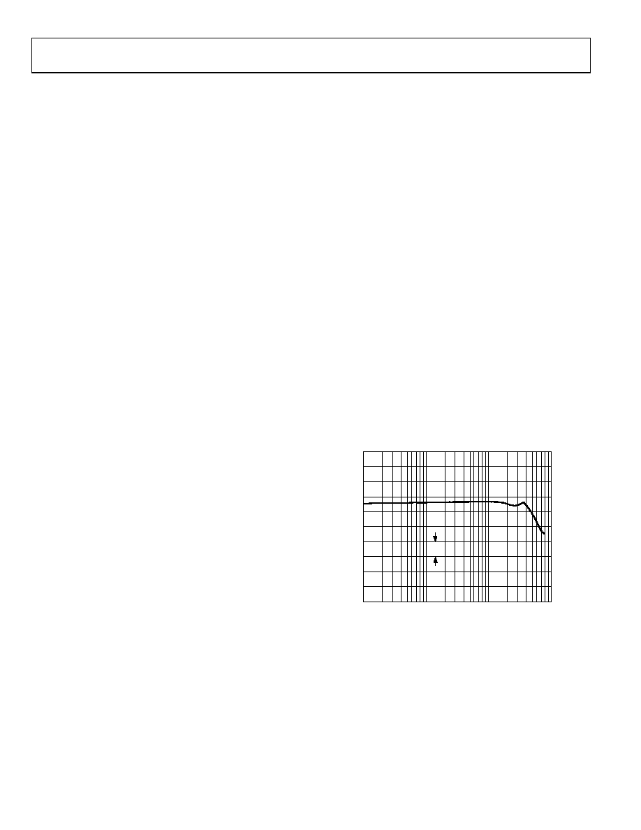
transistor can be used here to reduce HF peaking. Figure 38
shows the ac response at the stabilized output level of about
1.3 rms. Figure 39 demonstrates the output stabilization for the
sine wave inputs of 1 mV rms to 1 V rms at frequencies of 100 kHz,
1 MHz, and 10 MHz.
3dB
00
53
8-
0
36
Figure 38. AC Response at the Stabilized Output Level of 1.3 V rms
相关PDF资料 |
PDF描述 |
|---|---|
| UESD3.3DT5G | DIODE ESD PROTECT 3.3V SOT-723 |
| AMP01AX | IC AMP INST PREC LN 120MA 18CDIP |
| AD526CDZ | IC AMP PGA 10MA 16CDIP |
| AD585AQ | IC AMP SAMPLE HOLD 50MA 14CDIP |
| AD549KHZ | IC OPAMP GP 1MHZ LP 20MA TO99-8 |
相关代理商/技术参数 |
参数描述 |
|---|---|
| AD600ARZ1 | 制造商:AD 制造商全称:Analog Devices 功能描述:Dual, Low Noise, Wideband Variable Gain Amplifiers |
| AD600ARZ-R7 | 功能描述:IC AMP VGA DUAL LN 50MA 16SOIC RoHS:是 类别:集成电路 (IC) >> Linear - Amplifiers - Instrumentation 系列:X-AMP® 标准包装:2,500 系列:Excalibur™ 放大器类型:J-FET 电路数:1 输出类型:- 转换速率:45 V/µs 增益带宽积:10MHz -3db带宽:- 电流 - 输入偏压:20pA 电压 - 输入偏移:490µV 电流 - 电源:1.7mA 电流 - 输出 / 通道:48mA 电压 - 电源,单路/双路(±):4.5 V ~ 38 V,±2.25 V ~ 19 V 工作温度:-40°C ~ 85°C 安装类型:表面贴装 封装/外壳:8-SOIC(0.154",3.90mm 宽) 供应商设备封装:8-SOIC 包装:带卷 (TR) |
| AD600ARZ-RL | 功能描述:IC AMP VGA DUAL LN 50MA 16SOIC RoHS:是 类别:集成电路 (IC) >> Linear - Amplifiers - Instrumentation 系列:X-AMP® 标准包装:2,500 系列:Excalibur™ 放大器类型:J-FET 电路数:1 输出类型:- 转换速率:45 V/µs 增益带宽积:10MHz -3db带宽:- 电流 - 输入偏压:20pA 电压 - 输入偏移:490µV 电流 - 电源:1.7mA 电流 - 输出 / 通道:48mA 电压 - 电源,单路/双路(±):4.5 V ~ 38 V,±2.25 V ~ 19 V 工作温度:-40°C ~ 85°C 安装类型:表面贴装 封装/外壳:8-SOIC(0.154",3.90mm 宽) 供应商设备封装:8-SOIC 包装:带卷 (TR) |
| AD600EHDK42GIS | 制造商:Advanced Micro Devices 功能描述:EB E64 4C 600E AM3 45W - Trays |
| AD600EHDK42GMS | 制造商:Advanced Micro Devices 功能描述:EB E64 4C 600E AM3 45W - Trays |
发布紧急采购,3分钟左右您将得到回复。