参数资料
| 型号: | AD602AR-REEL |
| 厂商: | Analog Devices Inc |
| 文件页数: | 3/33页 |
| 文件大小: | 0K |
| 描述: | IC AMP VGA DUAL LN 50MA 16SOIC |
| 标准包装: | 1,000 |
| 系列: | X-AMP® |
| 放大器类型: | 可变增益 |
| 电路数: | 2 |
| 转换速率: | 275 V/µs |
| -3db带宽: | 35MHz |
| 电流 - 输入偏压: | 350nA |
| 电流 - 电源: | 11mA |
| 电流 - 输出 / 通道: | 50mA |
| 电压 - 电源,单路/双路(±): | ±4.75 V ~ 5.25 V |
| 工作温度: | -40°C ~ 85°C |
| 安装类型: | 表面贴装 |
| 封装/外壳: | 16-SOIC(0.295",7.50mm 宽) |
| 供应商设备封装: | 16-SOIC W |
| 包装: | 带卷 (TR) |
第1页第2页当前第3页第4页第5页第6页第7页第8页第9页第10页第11页第12页第13页第14页第15页第16页第17页第18页第19页第20页第21页第22页第23页第24页第25页第26页第27页第28页第29页第30页第31页第32页第33页
AD600/AD602
Rev. F | Page 10 of 32
THEORY OF OPERATION
The AD600/AD602 have the same general design and features.
They comprise two fixed gain amplifiers, each preceded by a
voltage-controlled attenuator of 0 dB to 42.14 dB with independent
control interfaces, each having a scaling factor of 32 dB per volt.
The AD600 amplifiers are laser trimmed to a gain of 41.07 dB
(×113), providing a control range of 1.07 dB to +41.07 dB
(0 dB to +40 dB with overlap). The AD602 amplifiers have a gain
of 31.07 dB (×35.8) and provide an overall gain of 11.07 dB to
+31.07 dB (10 dB to +30 dB with overlap).
The advantage of this topology is that the amplifier can use
negative feedback to increase the accuracy of its gain. In
addition, because the amplifier does not have to handle large
signals at its input, the distortion can be very low. Another
feature of this approach is that the small-signal gain and phase
response, and thus the pulse response, are essentially
independent of gain.
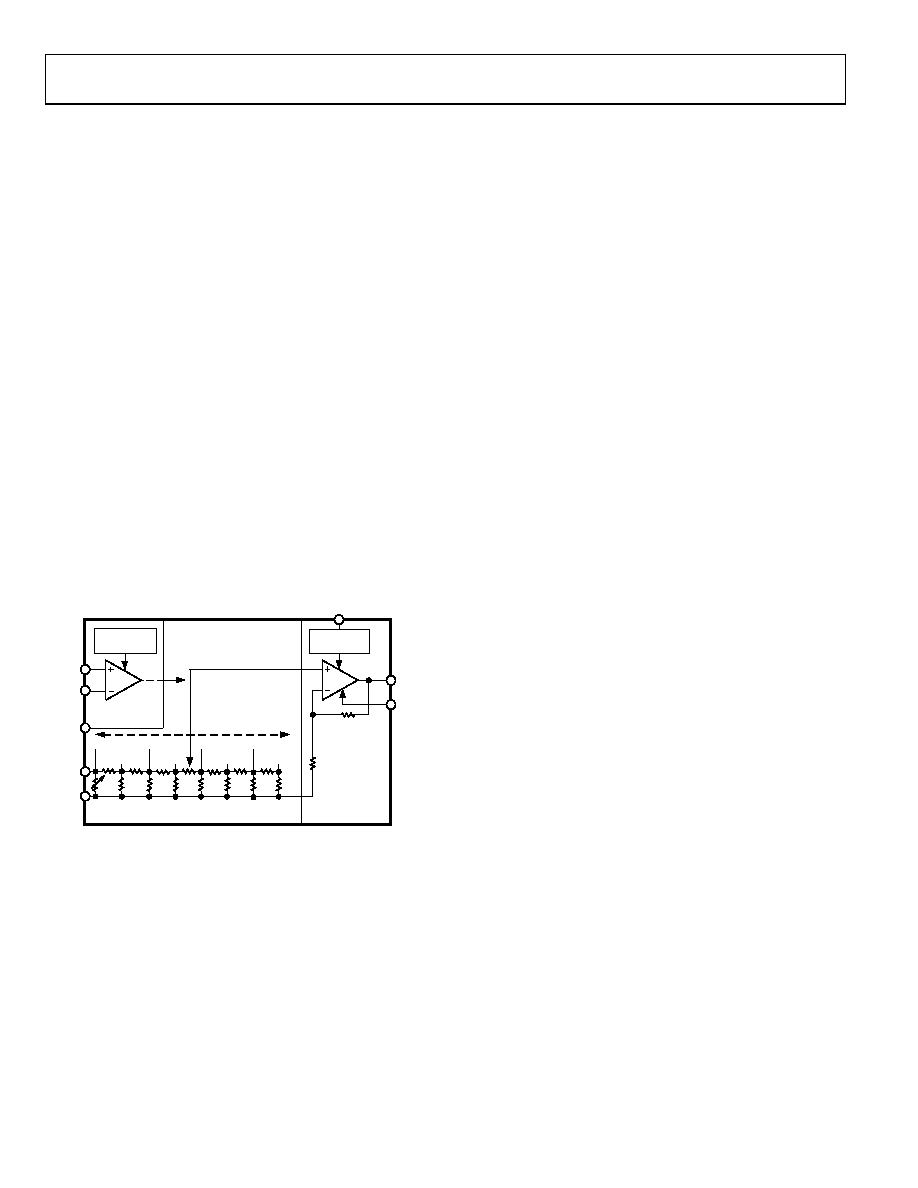
Figure 21 is a simplified schematic of one channel. The input
attenuator is a 7-stage R-2R ladder network, using untrimmed
resistors of nominally R = 62.5 Ω, which results in a characteristic
resistance of 125 Ω ± 20%. A shunt resistor is included at the
input and laser trimmed to establish a more exact input
resistance of 100 Ω ± 2%, which ensures accurate operation
(gain and HP corner frequency) when used in conjunction with
external resistors or capacitors.
PRECISION PASSIVE
INPUT ATTENUATOR
GATING
INTERFACE
SCALING
REFERENCE
GAT1
A1OP
A1CM
C1HI
C1LO
A1HI
A1LO
VG
GAIN CONTROL
INTERFACE
RF2
2.24k
(AD600)
694
(AD602)
RF1
20
FIXED-GAIN
AMPLIFIER
0dB
–6.02dB
–12.04dB
–18.06dB
–22.08dB
–30.1dB
–36.12dB
–42.14dB
R-2R LADDER NETWORK
41.07dB (AD600)
31.07dB (AD602)
500
62.5
00
53
8-
02
1
Figure 21. Simplified Block Diagram of a Single Channel of the AD600/AD602
The nominal maximum signal at input A1HI is 1 V rms (±1.4 V
peak) when using the recommended ±5 V supplies, although
operation to ±2 V peak is permissible with some increase in HF
distortion and feedthrough. Each attenuator is provided with a
separate signal LO connection for use in rejecting common
mode, the voltage between input and output grounds. Circuitry
is included to provide rejection of up to ±100 mV.
The signal applied at the input of the ladder network is
attenuated by 6.02 dB by each section; thus, the attenuation to
each of the taps is progressively 0 dB, 6.02 dB, 12.04 dB, 18.06 dB,
24.08 dB, 30.1 dB, 36.12 dB, and 42.14 dB. A unique circuit
technique is employed to interpolate between these tap points,
indicated by the slider in Figure 21, providing continuous
attenuation from 0 dB to 42.14 dB.
To understand the AD600/AD602, it helps to think in terms of
a mechanical means for moving this slider from left to right; in
fact, it is voltage controlled. The details of the control interface
are discussed later. Note that the gain is exactly determined at
all times and a linear decibel relationship is guaranteed auto-
matically between the gain and the control parameter that
determines the position of the slider. In practice, the gain
deviates from the ideal law by about ±0.2 dB peak (see Figure 28).
Note that the signal inputs are not fully differential. A1LO, A1CM
(for CH1), A2LO, and A2CM (for CH2) provide separate access
to the input and output grounds. This recognizes that, even when
using a ground plane, small differences arise in the voltages at
these nodes. It is important that A1LO and A2LO be connected
directly to the input ground(s). Significant impedance in these
connections reduces the gain accuracy. A1CM and A2CM
should be connected to the load ground(s).
NOISE PERFORMANCE
An important reason for using this approach is the superior
noise performance that can be achieved. The nominal resistance
seen at the inner tap points of the attenuator is 41.7 Ω (one third of
125 Ω), which, at 27°C, exhibits a Johnson noise spectral density
(NSD) of 0.84 nV/√Hz (that is, √4kTR), a large fraction of the
total input noise. The first stage of the amplifier contributes
another 1.12 nV/√Hz, for a total input noise of 1.4 nV/√Hz.
The noise at the 0 dB tap depends on whether the input is
short-circuited or open-circuited. When shorted, the minimum
NSD of 1.12 nV/√Hz is achieved. When open, the resistance of
100 Ω at the first tap generates 1.29 nV/√Hz, so the noise
increases to 1.71 nV/√Hz. This last calculation would be important
if the AD600 were preceded, for example, by a 900 Ω resistor to
allow operation from inputs up to ±10 V rms. However, in most
cases, the low impedance of the source limits the maximum
noise resistance.
相关PDF资料 |
PDF描述 |
|---|---|
| 69133-472HLF | BERGSTIK II .100" DR STRAIGHT |
| AD600AR-REEL | IC AMP VGA DUAL LN 50MA 16SOIC |
| MTSW-116-07-G-S-210 | CONN HEADER 16POS .100" STR GOLD |
| AD526BD | IC AMP PGA 10MA 16CDIP |
| TV02W180-G | TVS 200W 18V UNIDIRECT SOD-123 |
相关代理商/技术参数 |
参数描述 |
|---|---|
| AD602AR-REEL7 | 功能描述:IC AMP VGA DUAL LN 50MA 16SOIC RoHS:否 类别:集成电路 (IC) >> Linear - Amplifiers - Instrumentation 系列:X-AMP® 标准包装:2,500 系列:Excalibur™ 放大器类型:J-FET 电路数:1 输出类型:- 转换速率:45 V/µs 增益带宽积:10MHz -3db带宽:- 电流 - 输入偏压:20pA 电压 - 输入偏移:490µV 电流 - 电源:1.7mA 电流 - 输出 / 通道:48mA 电压 - 电源,单路/双路(±):4.5 V ~ 38 V,±2.25 V ~ 19 V 工作温度:-40°C ~ 85°C 安装类型:表面贴装 封装/外壳:8-SOIC(0.154",3.90mm 宽) 供应商设备封装:8-SOIC 包装:带卷 (TR) |
| AD602ARZ | 功能描述:IC AMP VGA DUAL LN 50MA 16SOIC RoHS:是 类别:集成电路 (IC) >> Linear - Amplifiers - Instrumentation 系列:X-AMP® 标准包装:1 系列:- 放大器类型:通用 电路数:4 输出类型:满摆幅 转换速率:0.028 V/µs 增益带宽积:105kHz -3db带宽:- 电流 - 输入偏压:3nA 电压 - 输入偏移:100µV 电流 - 电源:3.3µA 电流 - 输出 / 通道:12mA 电压 - 电源,单路/双路(±):2.7 V ~ 12 V,±1.35 V ~ 6 V 工作温度:-40°C ~ 85°C 安装类型:表面贴装 封装/外壳:14-TSSOP(0.173",4.40mm 宽) 供应商设备封装:14-TSSOP 包装:剪切带 (CT) 其它名称:OP481GRUZ-REELCT |
| AD602ARZ-R7 | 功能描述:IC AMP VGA DUAL LN 50MA 16SOIC RoHS:是 类别:集成电路 (IC) >> Linear - Amplifiers - Instrumentation 系列:X-AMP® 标准包装:2,500 系列:Excalibur™ 放大器类型:J-FET 电路数:1 输出类型:- 转换速率:45 V/µs 增益带宽积:10MHz -3db带宽:- 电流 - 输入偏压:20pA 电压 - 输入偏移:490µV 电流 - 电源:1.7mA 电流 - 输出 / 通道:48mA 电压 - 电源,单路/双路(±):4.5 V ~ 38 V,±2.25 V ~ 19 V 工作温度:-40°C ~ 85°C 安装类型:表面贴装 封装/外壳:8-SOIC(0.154",3.90mm 宽) 供应商设备封装:8-SOIC 包装:带卷 (TR) |
| AD602ARZ-RL | 功能描述:IC AMP VGA DUAL LN 50MA 16SOIC RoHS:是 类别:集成电路 (IC) >> Linear - Amplifiers - Instrumentation 系列:X-AMP® 标准包装:2,500 系列:Excalibur™ 放大器类型:J-FET 电路数:1 输出类型:- 转换速率:45 V/µs 增益带宽积:10MHz -3db带宽:- 电流 - 输入偏压:20pA 电压 - 输入偏移:490µV 电流 - 电源:1.7mA 电流 - 输出 / 通道:48mA 电压 - 电源,单路/双路(±):4.5 V ~ 38 V,±2.25 V ~ 19 V 工作温度:-40°C ~ 85°C 安装类型:表面贴装 封装/外壳:8-SOIC(0.154",3.90mm 宽) 供应商设备封装:8-SOIC 包装:带卷 (TR) |
| AD602J | 制造商:AD 制造商全称:Analog Devices 功能描述:Dual, Low Noise, Wideband Variable Gain Amplifiers |
发布紧急采购,3分钟左右您将得到回复。