参数资料
| 型号: | AD602AR-REEL |
| 厂商: | Analog Devices Inc |
| 文件页数: | 6/33页 |
| 文件大小: | 0K |
| 描述: | IC AMP VGA DUAL LN 50MA 16SOIC |
| 标准包装: | 1,000 |
| 系列: | X-AMP® |
| 放大器类型: | 可变增益 |
| 电路数: | 2 |
| 转换速率: | 275 V/µs |
| -3db带宽: | 35MHz |
| 电流 - 输入偏压: | 350nA |
| 电流 - 电源: | 11mA |
| 电流 - 输出 / 通道: | 50mA |
| 电压 - 电源,单路/双路(±): | ±4.75 V ~ 5.25 V |
| 工作温度: | -40°C ~ 85°C |
| 安装类型: | 表面贴装 |
| 封装/外壳: | 16-SOIC(0.295",7.50mm 宽) |
| 供应商设备封装: | 16-SOIC W |
| 包装: | 带卷 (TR) |
第1页第2页第3页第4页第5页当前第6页第7页第8页第9页第10页第11页第12页第13页第14页第15页第16页第17页第18页第19页第20页第21页第22页第23页第24页第25页第26页第27页第28页第29页第30页第31页第32页第33页
AD600/AD602
Rev. F | Page 13 of 32
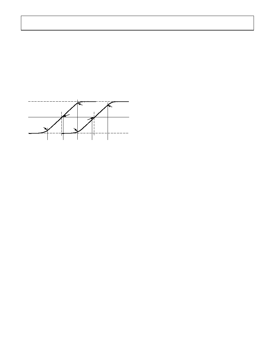
The gains are offset such that the gain of A2 is increased only
after the gain of A1 has reached its maximum value (see Figure 26).
Note that, for a differential input of 700 mV or less, the gain of
a single amplifier (A1 or A2) is at its minimum value of 1.07 dB;
for a differential input of +700 mV or more, the gain is at its
maximum value of +41.07 dB. Control inputs beyond these
limits do not affect the gain and can be tolerated without damage or
foldover in the response. See the Specifications section for more
details on the allowable voltage range. The gain is now
Gain (dB) = 32 VC
(3)
where VC is the applied control voltage.
+41.07dB
+20dB
+1.07dB
–0.56dB
–1.07dB
+40.56dB
+38.93dB
8
0
9
.
1
2
9
5
.
0
GAIN
(dB)
*GAIN OFFSET OF 1.07dB, OR 33.44mV
A1
A2
*
2.5
80
1.875
60
1.25
40
0.625
20
0
–2.14
VC (V)
82.14
00
53
8-
02
4
Figure 26. Explanation of Offset Calibration for Sequential Control
When VC is set to zero, VG1 = 0.592 V and the gain of A1 is
1.07 dB (recall that the gain of each amplifier section is 0 dB for
VG = 625 mV); meanwhile, VG2 = 1.908 V, so the gain of A2 is
1.07 dB. The overall gain is thus 0 dB (see Figure 23). When
VC = 1.25 V, VG1 = 1.25 V – 0.592 V = 0.658 V, which sets the
gain of A1 to 40.56 dB, while VG2 = 1.25 V – 1.908 V = 0.658 V,
which sets the gain of A2 at 0.56 dB. The overall gain is now
and the gain of A2 is 38.93 dB, resulting in an overall gain of 80
dB (see Figure 25). This mode of operation is further clarified
by Figure 27, which is a plot of the separate gains of A1 and A2
and the overall gain vs. the control voltage. Figure 28 is a plot of
the gain error of the cascaded amplifiers vs. the control voltage.
PARALLEL MODE (SIMPLEST GAIN-CONTROL
INTERFACE)
In this mode, the gain-control voltage is applied to both inputs
in parallel—C1HI and C2HI are connected to the control
voltage, and C1LO and C2LO are optionally connected to an
offset voltage of 0.625 V. The gain scaling is then doubled to
64dB/V, requiring only 1.25 V for an 80 dB change of gain. In
this case, the amplitude of the gain ripple is also doubled, as is
shown in Figure 29, and the instantaneous SNR at the output of
A2 decreases linearly as the gain is increased (see Figure 30).
LOW RIPPLE MODE (MINIMUM GAIN ERROR)
As shown in Figure 28 and Figure 29, the output ripple is
periodic. By offsetting the gains of A1 and A2 by half the
period of the ripple, or 3 dB, the residual gain errors of the two
amplifiers can be made to cancel. Figure 31 shows the much
lower gain ripple when configured in this manner. Figure 32
plots the SNR as a function of gain; it is very similar to that in
the parallel mode.
相关PDF资料 |
PDF描述 |
|---|---|
| 69133-472HLF | BERGSTIK II .100" DR STRAIGHT |
| AD600AR-REEL | IC AMP VGA DUAL LN 50MA 16SOIC |
| MTSW-116-07-G-S-210 | CONN HEADER 16POS .100" STR GOLD |
| AD526BD | IC AMP PGA 10MA 16CDIP |
| TV02W180-G | TVS 200W 18V UNIDIRECT SOD-123 |
相关代理商/技术参数 |
参数描述 |
|---|---|
| AD602AR-REEL7 | 功能描述:IC AMP VGA DUAL LN 50MA 16SOIC RoHS:否 类别:集成电路 (IC) >> Linear - Amplifiers - Instrumentation 系列:X-AMP® 标准包装:2,500 系列:Excalibur™ 放大器类型:J-FET 电路数:1 输出类型:- 转换速率:45 V/µs 增益带宽积:10MHz -3db带宽:- 电流 - 输入偏压:20pA 电压 - 输入偏移:490µV 电流 - 电源:1.7mA 电流 - 输出 / 通道:48mA 电压 - 电源,单路/双路(±):4.5 V ~ 38 V,±2.25 V ~ 19 V 工作温度:-40°C ~ 85°C 安装类型:表面贴装 封装/外壳:8-SOIC(0.154",3.90mm 宽) 供应商设备封装:8-SOIC 包装:带卷 (TR) |
| AD602ARZ | 功能描述:IC AMP VGA DUAL LN 50MA 16SOIC RoHS:是 类别:集成电路 (IC) >> Linear - Amplifiers - Instrumentation 系列:X-AMP® 标准包装:1 系列:- 放大器类型:通用 电路数:4 输出类型:满摆幅 转换速率:0.028 V/µs 增益带宽积:105kHz -3db带宽:- 电流 - 输入偏压:3nA 电压 - 输入偏移:100µV 电流 - 电源:3.3µA 电流 - 输出 / 通道:12mA 电压 - 电源,单路/双路(±):2.7 V ~ 12 V,±1.35 V ~ 6 V 工作温度:-40°C ~ 85°C 安装类型:表面贴装 封装/外壳:14-TSSOP(0.173",4.40mm 宽) 供应商设备封装:14-TSSOP 包装:剪切带 (CT) 其它名称:OP481GRUZ-REELCT |
| AD602ARZ-R7 | 功能描述:IC AMP VGA DUAL LN 50MA 16SOIC RoHS:是 类别:集成电路 (IC) >> Linear - Amplifiers - Instrumentation 系列:X-AMP® 标准包装:2,500 系列:Excalibur™ 放大器类型:J-FET 电路数:1 输出类型:- 转换速率:45 V/µs 增益带宽积:10MHz -3db带宽:- 电流 - 输入偏压:20pA 电压 - 输入偏移:490µV 电流 - 电源:1.7mA 电流 - 输出 / 通道:48mA 电压 - 电源,单路/双路(±):4.5 V ~ 38 V,±2.25 V ~ 19 V 工作温度:-40°C ~ 85°C 安装类型:表面贴装 封装/外壳:8-SOIC(0.154",3.90mm 宽) 供应商设备封装:8-SOIC 包装:带卷 (TR) |
| AD602ARZ-RL | 功能描述:IC AMP VGA DUAL LN 50MA 16SOIC RoHS:是 类别:集成电路 (IC) >> Linear - Amplifiers - Instrumentation 系列:X-AMP® 标准包装:2,500 系列:Excalibur™ 放大器类型:J-FET 电路数:1 输出类型:- 转换速率:45 V/µs 增益带宽积:10MHz -3db带宽:- 电流 - 输入偏压:20pA 电压 - 输入偏移:490µV 电流 - 电源:1.7mA 电流 - 输出 / 通道:48mA 电压 - 电源,单路/双路(±):4.5 V ~ 38 V,±2.25 V ~ 19 V 工作温度:-40°C ~ 85°C 安装类型:表面贴装 封装/外壳:8-SOIC(0.154",3.90mm 宽) 供应商设备封装:8-SOIC 包装:带卷 (TR) |
| AD602J | 制造商:AD 制造商全称:Analog Devices 功能描述:Dual, Low Noise, Wideband Variable Gain Amplifiers |
发布紧急采购,3分钟左右您将得到回复。