- 您现在的位置:买卖IC网 > PDF目录16923 > AD604-EVALZ (Analog Devices Inc)BOARD EVAL FOR AD604 AMP PDF资料下载
参数资料
| 型号: | AD604-EVALZ |
| 厂商: | Analog Devices Inc |
| 文件页数: | 15/33页 |
| 文件大小: | 0K |
| 描述: | BOARD EVAL FOR AD604 AMP |
| 标准包装: | 1 |
| 系列: | X-AMP® |
| 每 IC 通道数: | 2 - 双 |
| 放大器类型: | 可变增益 |
| 输出类型: | 单端 |
| 转换速率: | 170 V/µs |
| -3db带宽: | 40MHz |
| 电流 - 输出 / 通道: | 40mA |
| 工作温度: | -40°C ~ 85°C |
| 电流供应(主 IC): | 32mA |
| 板类型: | 完全填充 |
| 已供物品: | 板 |
| 已用 IC / 零件: | AD604 |
| 相关产品: | AD604ARZ-RL-ND - IC AMP VGA DUAL ULN 40MA 24SOIC AD604ANZ-ND - IC AMP VGA DUAL ULN 40MA 24DIP AD604ARSZ-R7-ND - IC AMP VGA DUAL ULN 40MA 24SSOP AD604ARSZ-RL-ND - IC AMP VGA DUAL ULN 40MA 24SSOP AD604ARSZ-ND - IC AMP VGA DUAL ULN 40MA 24SSOP AD604ARZ-ND - IC AMP VGA DUAL ULN 40MA 24SOIC AD604AR-REEL-ND - IC AMP VGA DUAL ULN 40MA 24SOIC AD604AR-ND - IC AMP VGA DUAL ULN 40MA 24SOIC |
第1页第2页第3页第4页第5页第6页第7页第8页第9页第10页第11页第12页第13页第14页当前第15页第16页第17页第18页第19页第20页第21页第22页第23页第24页第25页第26页第27页第28页第29页第30页第31页第32页第33页
AD604
Rev. G | Page 21 of 32
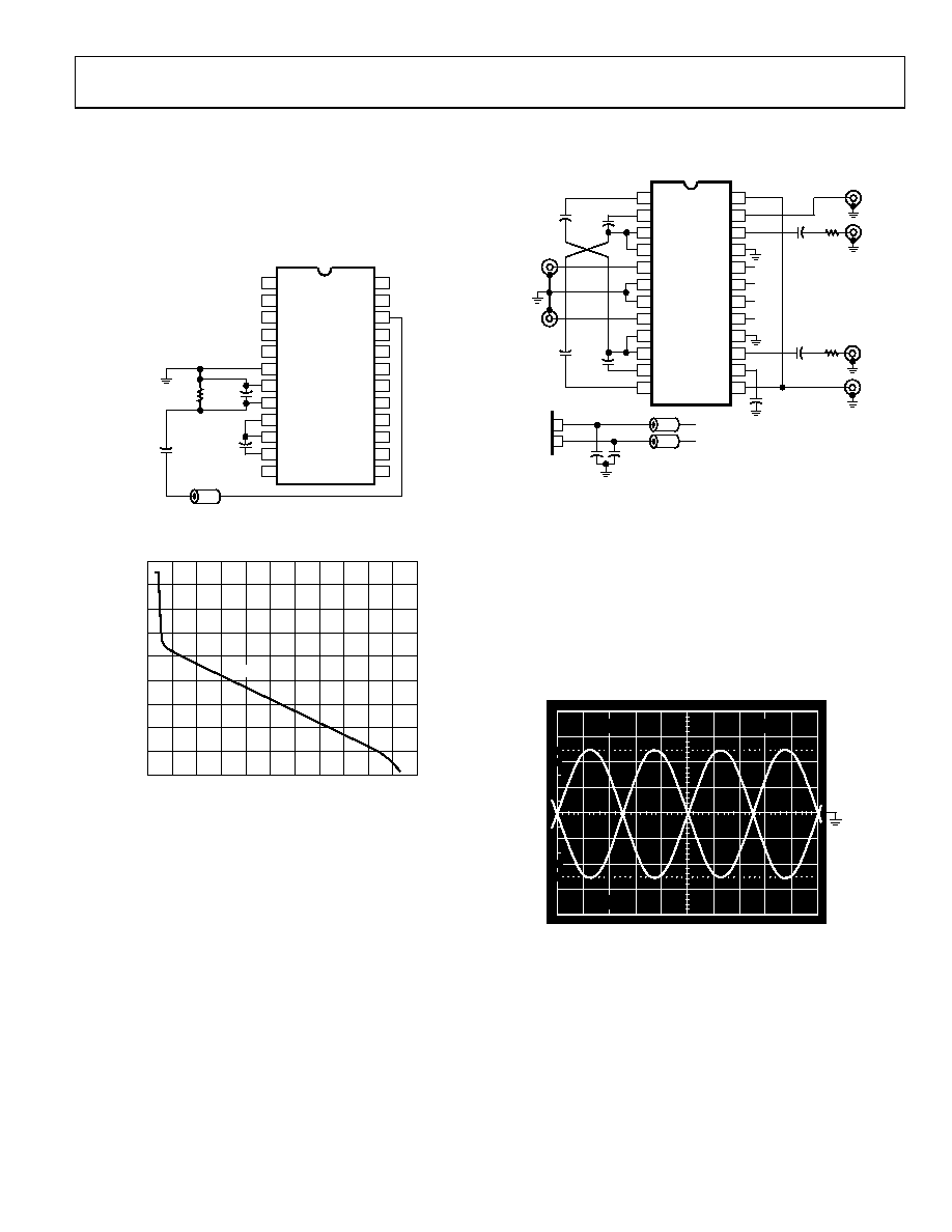
At 1 MHz, the attenuation is about 0.2 dB, increasing to 6 dB
at 10 MHz and 28 dB at 100 MHz. Signals less than approximately
1 MHz are not significantly affected.
Figure 49 shows the control voltage vs. the input power at 1 MHz
to the circuit shown in Figure 48; note that the AGC threshold is at
95 dBm. The output signal level is set to 800 mV p-p by applying
80 mV to the VSET connector.
12
11
10
9
8
1
2
3
4
7
6
5
13
16
15
14
24
23
22
21
20
19
18
17
AD604
FB
–DSX1
+DSX1
PAI1
FBK1
PAO1
COM1
COM2
PAI2
FBK2
PAO2
+DSX2
–DSX2
VGN1
VREF
VPOS
GND1
OUT1
VNEG
VPOS
GND2
OUT2
VOCM
VGN2
FAIR-RITE
#2643000301
C5
0.1F
R2
499
C6
560pF
C3
0.1F
00
54
0-
04
8
Figure 48. Modifications of the AGC Amplifier to Create 96 dB of Gain Range
4.5
4.0
0
3.5
3.0
1.0
2.5
2.0
1.5
CO
NT
R
O
L
V
O
L
T
AG
E
(V
)
1MHz
0.5
PIN (dBm)
–100 –90 –80 –70 –60 –50 –40 –30 –20 –10
0
10
00
54
0-
0
49
Figure 49. Control Voltage vs. Input Power of the Circuit in Figure 48
ULTRALOW NOISE, DIFFERENTIAL INPUT-
DIFFERENTIAL OUTPUT VGA
Figure 50 shows how to use both preamplifiers and DSXs to
create a high impedance, differential input-differential output
VGA. This application takes advantage of the differential inputs
to the DSXs. Note that the input is not truly differential in the
sense that the common-mode voltage needs to be at ground to
achieve maximum input signal swing. This has largely to do
with the limited output swing capability of the output drivers of
the preamplifiers; they clip around ±2.2 V due to having to drive
an effective load of about 30 Ω. If a different input common-mode
voltage needs to be accommodated, ac coupling (as in Figure 48)
is recommended. The differential gain range of this circuit runs
from 6 dB to 54 dB, which is 6 dB higher than each individual
the signal amplitude compared with when they are driven
single-ended.
13
16
15
14
19
18
17
24
23
22
21
20
12
11
10
9
8
1
2
3
4
7
6
5
AD604
FB
+5V
–5V
ALL SUPPLY PINS ARE DECOUPLED AS SHOWN.
+5V
–5V
+5V
VIN+
VIN–
VG
VREF
VOUT+
VOUT–
–DSX1
+DSX1
PAI1
FBK1
PAO1
COM1
COM2
PAI2
FBK2
PAO2
+DSX2
–DSX2
VGN1
VREF
VPOS
GND1
OUT1
VNEG
VPOS
GND2
OUT2
VOCM
VGN2
C13
0.1F
C12
0.1F
C1
0.1F
C2
0.1F
C4
0.1F
C3
0.1F
C5
0.1F
C7
0.1F
R1
453
R2
453
C6
0.1F
005
40-
05
0
Figure 50. Ultralow Noise, Differential Input-Differential Output VGA
Fig
r
,
ure 51 displays the output signals VOUT+ and VOUT afte
a 20 dB attenuator formed between the 453 Ω resistors shown
in Figure 50 and the 50 Ω loads presented by the oscilloscope
plug-in. R1 and R2 are inserted to ensure a nominal load of 500 Ω
at each output. The differential gain of the circuit is set to 20 dB
by applying a control voltage, VGN, of 1 V; the gain scaling is
20 dB/V for a VREF of 2.500 V; the input frequency is 10 MHz
and the differential input amplitude is 100 mV p-p. The resulting
differential output amplitude is 1 V p-p as can be seen on the
scope photo when reading the vertical scale as 200 mV/div.
10
0%
100
90
20ns
20mV
NOTES
1. THE OUTPUT AFTER 10× ATTENUATER FORMED
BY 453 TOGETHER WITH 50 OF 7A24 PLUG-IN.
–500mV
ACTUAL
VOUT
+500mV
0
05
40-
054
Figure 51. Output of VGA in Figure 50 for VGN = 1 V
channel of the AD604 because the DSX inputs now see twice
相关PDF资料 |
PDF描述 |
|---|---|
| MIC2566-1YM | IC PCMCIA/CARDBUS SGL 14-SOP |
| AD8337-EVALZ-SS | BOARD EVALUATION FOR AD8337 SS |
| AD8264-EVALZ | BOARD EVAL FOR AD8264 VGA |
| X60003BIG3Z-50T1 | IC VREF SERIES PREC 5V SOT-23-3 |
| 381LX471M450A052 | CAP ALUM 470UF 450V 20% SNAP |
相关代理商/技术参数 |
参数描述 |
|---|---|
| AD605 | 制造商:Analog Devices 功能描述: |
| AD605_06 | 制造商:AD 制造商全称:Analog Devices 功能描述:Dual, Low Noise, Single-Supply Variable Gain Amplifier |
| AD605_07 | 制造商:AD 制造商全称:Analog Devices 功能描述:Dual, Low Noise, Single-Supply Variable Gain Amplifier |
| AD605-00E | 功能描述:SENSOR MAG SW 40G STANDRD 8-MSOP 制造商:nve corp/sensor products 系列:AD 包装:管件 零件状态:有效 功能:全极开关 技术:霍尔效应 极化:任意一种 感应范围:±5mT 跳闸,±2.5mT 释放 测试条件:-40°C ~ 125°C 电压 - 电源:4.5 V ~ 30 V 电流 - 电源(最大值):4.5mA 电流 - 输出(最大值):20mA 输出类型:开路集电极 特性:- 工作温度:-40°C ~ 125°C(TA) 封装/外壳:8-TSSOP,8-MSOP(0.118",3.00mm 宽) 供应商器件封装:8-MSOP 标准包装:1,000 |
| AD605-02E | 功能描述:SENSOR MAG SW 40G STANDARD 8SOIC 制造商:nve corp/sensor products 系列:AD 包装:管件 零件状态:有效 功能:全极开关 技术:霍尔效应 极化:任意一种 感应范围:±5mT 跳闸,±2.5mT 释放 测试条件:-40°C ~ 125°C 电压 - 电源:4.5 V ~ 30 V 电流 - 电源(最大值):4.5mA 电流 - 输出(最大值):20mA 输出类型:开路集电极 特性:- 工作温度:-40°C ~ 125°C(TA) 封装/外壳:8-SOIC(0.154",3.90mm 宽) 供应商器件封装:8-SOIC 标准包装:1,000 |
发布紧急采购,3分钟左右您将得到回复。