- 您现在的位置:买卖IC网 > PDF目录16923 > AD604-EVALZ (Analog Devices Inc)BOARD EVAL FOR AD604 AMP PDF资料下载
参数资料
| 型号: | AD604-EVALZ |
| 厂商: | Analog Devices Inc |
| 文件页数: | 6/33页 |
| 文件大小: | 0K |
| 描述: | BOARD EVAL FOR AD604 AMP |
| 标准包装: | 1 |
| 系列: | X-AMP® |
| 每 IC 通道数: | 2 - 双 |
| 放大器类型: | 可变增益 |
| 输出类型: | 单端 |
| 转换速率: | 170 V/µs |
| -3db带宽: | 40MHz |
| 电流 - 输出 / 通道: | 40mA |
| 工作温度: | -40°C ~ 85°C |
| 电流供应(主 IC): | 32mA |
| 板类型: | 完全填充 |
| 已供物品: | 板 |
| 已用 IC / 零件: | AD604 |
| 相关产品: | AD604ARZ-RL-ND - IC AMP VGA DUAL ULN 40MA 24SOIC AD604ANZ-ND - IC AMP VGA DUAL ULN 40MA 24DIP AD604ARSZ-R7-ND - IC AMP VGA DUAL ULN 40MA 24SSOP AD604ARSZ-RL-ND - IC AMP VGA DUAL ULN 40MA 24SSOP AD604ARSZ-ND - IC AMP VGA DUAL ULN 40MA 24SSOP AD604ARZ-ND - IC AMP VGA DUAL ULN 40MA 24SOIC AD604AR-REEL-ND - IC AMP VGA DUAL ULN 40MA 24SOIC AD604AR-ND - IC AMP VGA DUAL ULN 40MA 24SOIC |
第1页第2页第3页第4页第5页当前第6页第7页第8页第9页第10页第11页第12页第13页第14页第15页第16页第17页第18页第19页第20页第21页第22页第23页第24页第25页第26页第27页第28页第29页第30页第31页第32页第33页
AD604
Rev. G | Page 13 of 32
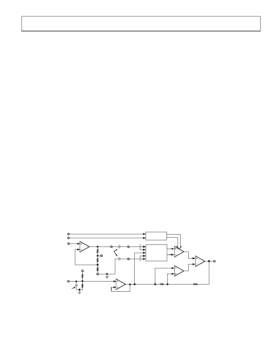
THEORY OF OPERATION
The AD604 is a dual-channel VGA with an ultralow noise
preamplifier. Figure 37 shows the simplified block diagram of
one channel. Each identical channel consists of a preamplifier
with gain setting resistors (R5, R6, and R7) and a single-supply
X-AMP (hereafter called DSX, differential single-supply X-AMP)
made up of the following:
A precision passive attenuator (differential ladder).
A gain control block.
A VOCM buffer with supply splitting resistors
(R3 and R4).
An active feedback amplifier (AFA) with gain setting
resistors (R1 and R2). To understand the active-feedback
amplifier topology, refer to the AD830 data sheet. The
AD830 is a practical implementation of the idea.
The preamplifier is powered by a ±5 V supply, while the DSX
uses a single +5 V supply. The linear-in-dB gain response of the
AD604 can generally be described by
G (dB) = Gain Scaling (dB/V) × Gain Control (V) +
(Preamp Gain (dB) 19 dB)
(1)
Each channel provides between 0 dB to 48.4 dB and 6 dB to 54.4
dB of gain, depending on the user-determined preamplifier
gain. The center 40 dB of gain is exactly linear-in-dB while the
gain error increases at the top and bottom of the range. The gain
of the preamplifier is typically either 14 dB or 20 dB but can be
set to intermediate values by a single external resistor (see the
Preamplifier section for details). The gain of the DSX can vary
from 14 dB to +34.4 dB, as determined by the gain control
voltage (VGN). The VREF input establishes the gain scaling;
the useful gain scaling range is between 20 dB/V and 40 dB/V
for a VREF voltage of 2.5 V and 1.25 V, respectively. For
example, if the preamp gain is set to 14 dB and VREF is set to
2.50 V (to establish a gain scaling of 20 dB/V), the gain equation
simplifies to
G (dB) = 20 (dB/V) × VGN (V) – 5 dB
The desired gain can then be achieved by setting the unipolar
gain control (VGN) to a voltage within its nominal operating
range of 0.25 V to 2.65 V (for 20 dB/V gain scaling). The gain is
monotonic for a complete gain control voltage range of 0.1 V to
2.9 V. Maximum gain can be achieved at a VGN of 2.9 V.
The inputs VREF and VOCM are common to both channels.
They are decoupled to ground, minimizing interchannel
crosstalk. For the highest gain scaling accuracy, VREF should
have an external low impedance voltage source. For low accuracy
20 dB/V applications, the VREF input can be decoupled with a
capacitor to ground. In this mode, the gain scaling is determined
by the midpoint between VPOS and GND; therefore, care
should be taken to control the supply voltage to 5 V. The input
resistance looking into the VREF pin is 10 kΩ ± 20%.
The DSX portion of the AD604 is a single-supply circuit, and
the VOCM pin is used to establish the dc level of the midpoint
of this portion of the circuit. The VOCM pin only needs an
external decoupling capacitor to ground to center the midpoint
between the supply voltages (5 V, GND); however, the VOCM
can be adjusted to other voltage levels if the dc common-mode
level of the output is important to the user (for example, see the
section entitled Medical Ultrasound TGC Driving the AD9050,
a 10-Bit, 40 MSPS ADC). The input resistance looking into the
VOCM pin is 45 kΩ ± 20%.
FBKx
C1
VGNx
PAIx
–DSXx
EXT.
COMx
VPOS
VOCM
C3
C2
OUTx
175
G1
Ao
G2
EXT.
175
R4
200k
R3
200k
VREF
DISTRIBUTED GM
GAIN
CONTROL
DIFFERENTIAL
ATTENUATOR
R1
820
R2
20
+DSXx
PAOx
R7
40
R5
32
R6
8
005
40
-03
7
Figure 37. Simplified Block Diagram of a Single Channel of the AD604
相关PDF资料 |
PDF描述 |
|---|---|
| MIC2566-1YM | IC PCMCIA/CARDBUS SGL 14-SOP |
| AD8337-EVALZ-SS | BOARD EVALUATION FOR AD8337 SS |
| AD8264-EVALZ | BOARD EVAL FOR AD8264 VGA |
| X60003BIG3Z-50T1 | IC VREF SERIES PREC 5V SOT-23-3 |
| 381LX471M450A052 | CAP ALUM 470UF 450V 20% SNAP |
相关代理商/技术参数 |
参数描述 |
|---|---|
| AD605 | 制造商:Analog Devices 功能描述: |
| AD605_06 | 制造商:AD 制造商全称:Analog Devices 功能描述:Dual, Low Noise, Single-Supply Variable Gain Amplifier |
| AD605_07 | 制造商:AD 制造商全称:Analog Devices 功能描述:Dual, Low Noise, Single-Supply Variable Gain Amplifier |
| AD605-00E | 功能描述:SENSOR MAG SW 40G STANDRD 8-MSOP 制造商:nve corp/sensor products 系列:AD 包装:管件 零件状态:有效 功能:全极开关 技术:霍尔效应 极化:任意一种 感应范围:±5mT 跳闸,±2.5mT 释放 测试条件:-40°C ~ 125°C 电压 - 电源:4.5 V ~ 30 V 电流 - 电源(最大值):4.5mA 电流 - 输出(最大值):20mA 输出类型:开路集电极 特性:- 工作温度:-40°C ~ 125°C(TA) 封装/外壳:8-TSSOP,8-MSOP(0.118",3.00mm 宽) 供应商器件封装:8-MSOP 标准包装:1,000 |
| AD605-02E | 功能描述:SENSOR MAG SW 40G STANDARD 8SOIC 制造商:nve corp/sensor products 系列:AD 包装:管件 零件状态:有效 功能:全极开关 技术:霍尔效应 极化:任意一种 感应范围:±5mT 跳闸,±2.5mT 释放 测试条件:-40°C ~ 125°C 电压 - 电源:4.5 V ~ 30 V 电流 - 电源(最大值):4.5mA 电流 - 输出(最大值):20mA 输出类型:开路集电极 特性:- 工作温度:-40°C ~ 125°C(TA) 封装/外壳:8-SOIC(0.154",3.90mm 宽) 供应商器件封装:8-SOIC 标准包装:1,000 |
发布紧急采购,3分钟左右您将得到回复。