参数资料
| 型号: | AD621BNZ |
| 厂商: | Analog Devices Inc |
| 文件页数: | 3/16页 |
| 文件大小: | 0K |
| 描述: | IC AMP INST LDRIFT LP 18MA 8DIP |
| 产品培训模块: | Instrumentation Amplifiers Performance |
| 标准包装: | 50 |
| 放大器类型: | 仪表 |
| 电路数: | 1 |
| 转换速率: | 1.2 V/µs |
| -3db带宽: | 800kHz |
| 电流 - 输入偏压: | 500pA |
| 电压 - 输入偏移: | 50µV |
| 电流 - 电源: | 900µA |
| 电流 - 输出 / 通道: | 18mA |
| 电压 - 电源,单路/双路(±): | ±2.3 V ~ 18 V |
| 工作温度: | -40°C ~ 85°C |
| 安装类型: | 通孔 |
| 封装/外壳: | 8-DIP(0.300",7.62mm) |
| 供应商设备封装: | 8-PDIP |
| 包装: | 管件 |
| 产品目录页面: | 770 (CN2011-ZH PDF) |
AD621
REV. B
–11–
–
+
AD705
5V
3k
AD621B
ADC
REF
IN
AGND
DIGITAL
DATA
OUTPUT
20k
10k
20k
–
+
0.6mA
MAX
0.10mA
1.3mA
MAX
1.7mA
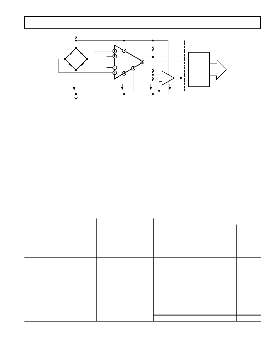
Figure 5. A Pressure Monitor Circuit which Operates on a 5 V Power Supply
Pressure Measurement
Although useful in many bridge applications such as weigh-scales,
the AD621 is especially suited for higher resistance pressure
sensors powered at lower voltages where small size and low
power become more even significant.
Figure 5 shows a 3 k
pressure transducer bridge powered from
5 V. In such a circuit, the bridge consumes only 1.7 mA. Adding
the AD621 and a buffered voltage divider allows the signal to be
conditioned for only 3.8 mA of total supply current.
Small size and low cost make the AD621 especially attractive for
voltage output pressure transducers. Since it delivers low noise
and drift, it will also serve applications such as diagnostic non-
invasion blood pressure measurement.
Wide Dynamic Range Gain Block Suppresses Large Common-
Mode and Offset Signals
The AD621 is especially useful in wide dynamic range applica-
tions such as those requiring the amplification of signals in the
presence of large, unwanted common-mode signals or offsets.
Many monolithic in amps achieve low total input drift and noise
errors only at relatively high gains (~100). In contrast the AD621’s
low output errors allow such performance at a gain of 10, thus
allowing larger input signals and therefore greater dynamic
range. The circuit of Figure 6 (
± 15 V supply, G = 10) has
only 2.5
V/°C max. VOS drift and 0.55 /V p-p typical 0.1 Hz
to 10 Hz noise, yet will amplify a
±0.5 V differential signal while
suppressing a
±10 V common-mode signal, or it will amplify a
±1.25 V differential signal while suppressing a 1 V offset by use
of the DAC driving the reference pin of the AD621. An added
benefit, the offsetting DAC connected to the reference pin allows
removal of a dc signal without the associated time-constant
of ac coupling. Note the representations of a differential and
common-mode signal shown in Figure 6 such that a single-ended
(or normal mode) signal of 1 V would be composed of a 0.5 V
common-mode component and a 1 V differential component.
Table I. Make vs. Buy Error Budget
AD621 Circuit
Discrete Circuit
Error, ppm of Full Scale
Error Source
Calculation
AD621
Discrete
ABSOLUTE ACCURACY at TA = +25
°C
Input Offset Voltage,
V
125
V/20 mV
(150
V × 2/20 mV
16,250
15,000
Output Offset Voltage,
V
N/A
((150
V × 2)/100)/20 mV
N/A
12,150
Input Offset Current, nA
2 nA
× 350 /20 mV
(6 nA
× 350 )/20 mV
12,118
121,53
CMR, dB
110 dB
→3.16 ppm, × 5 V/20 mV (0.02% Match × 5 V)/20 mV
12,791
14,988
Total Absolute Error
17,558
20,191
DRIFT TO +85
°C
Gain Drift, ppm/
°C
5 ppm
× 60°C
100 ppm/
°C Track × 60°C
13,300
12,600
Input Offset Voltage Drift,
V/°C1 V/°C × 60°C/20 mV
(2.5
V/°C × 2 × 60°C)/20 mV
13,000
15,000
Output Offset Voltage Drift,
V/°C
N/A
(2.5
V/°C × 2 × 60°C)/100/20 mV
N/A
12,150
Total Drift Error
13,690
15,750
RESOLUTION
Gain Nonlinearity, ppm of Full Scale
40 ppm
12,140
Typ 0.1 Hz–10 Hz Voltage Noise,
V p-p 0.28 V p-p/20 mV
(0.38
V p-p × √2)120 mV
121,14
12,127
Total Resolution Error
121,54
121,67
Grand Total Error
11,472
36,008
G = 100, VS =
± 15 V.
(All errors are min/max and referred to input.)
相关PDF资料 |
PDF描述 |
|---|---|
| 929500-01-21-RK | CONN HEADER .100 SNGL R/A 21POS |
| LT1230CS#PBF | IC CURR FEEDBACK AMP QUAD 14SOIC |
| RMCF0603JT56R0 | RES 56 OHM 1/10W 5% 0603 SMD |
| GEC10SGSN-M89 | CONN HEADER 10POS .100 RT/A SMD |
| PBC11DFAN | CONN HEADER .100 DUAL STR 22POS |
相关代理商/技术参数 |
参数描述 |
|---|---|
| AD621BR | 功能描述:IC AMP INST LDRIFT LP 18MA 8SOIC RoHS:否 类别:集成电路 (IC) >> Linear - Amplifiers - Instrumentation 系列:- 标准包装:50 系列:- 放大器类型:J-FET 电路数:2 输出类型:- 转换速率:3.5 V/µs 增益带宽积:1MHz -3db带宽:- 电流 - 输入偏压:30pA 电压 - 输入偏移:2000µV 电流 - 电源:200µA 电流 - 输出 / 通道:- 电压 - 电源,单路/双路(±):7 V ~ 36 V,±3.5 V ~ 18 V 工作温度:0°C ~ 70°C 安装类型:通孔 封装/外壳:8-DIP(0.300",7.62mm) 供应商设备封装:8-PDIP 包装:管件 |
| AD621BR-REEL | 功能描述:IC AMP INST LDRIFT LP 18MA 8SOIC RoHS:否 类别:集成电路 (IC) >> Linear - Amplifiers - Instrumentation 系列:- 标准包装:2,500 系列:Excalibur™ 放大器类型:J-FET 电路数:1 输出类型:- 转换速率:45 V/µs 增益带宽积:10MHz -3db带宽:- 电流 - 输入偏压:20pA 电压 - 输入偏移:490µV 电流 - 电源:1.7mA 电流 - 输出 / 通道:48mA 电压 - 电源,单路/双路(±):4.5 V ~ 38 V,±2.25 V ~ 19 V 工作温度:-40°C ~ 85°C 安装类型:表面贴装 封装/外壳:8-SOIC(0.154",3.90mm 宽) 供应商设备封装:8-SOIC 包装:带卷 (TR) |
| AD621BR-REEL7 | 功能描述:IC AMP INST LDRIFT LP 18MA 8SOIC RoHS:否 类别:集成电路 (IC) >> Linear - Amplifiers - Instrumentation 系列:- 标准包装:2,500 系列:Excalibur™ 放大器类型:J-FET 电路数:1 输出类型:- 转换速率:45 V/µs 增益带宽积:10MHz -3db带宽:- 电流 - 输入偏压:20pA 电压 - 输入偏移:490µV 电流 - 电源:1.7mA 电流 - 输出 / 通道:48mA 电压 - 电源,单路/双路(±):4.5 V ~ 38 V,±2.25 V ~ 19 V 工作温度:-40°C ~ 85°C 安装类型:表面贴装 封装/外壳:8-SOIC(0.154",3.90mm 宽) 供应商设备封装:8-SOIC 包装:带卷 (TR) |
| AD621BRZ | 功能描述:IC AMP INST LDRIFT LP 18MA 8SOIC RoHS:是 类别:集成电路 (IC) >> Linear - Amplifiers - Instrumentation 系列:- 标准包装:50 系列:- 放大器类型:J-FET 电路数:2 输出类型:- 转换速率:3.5 V/µs 增益带宽积:1MHz -3db带宽:- 电流 - 输入偏压:30pA 电压 - 输入偏移:2000µV 电流 - 电源:200µA 电流 - 输出 / 通道:- 电压 - 电源,单路/双路(±):7 V ~ 36 V,±3.5 V ~ 18 V 工作温度:0°C ~ 70°C 安装类型:通孔 封装/外壳:8-DIP(0.300",7.62mm) 供应商设备封装:8-PDIP 包装:管件 |
| AD621BRZ | 制造商:Analog Devices 功能描述:IC, INSTRUMENT AMP, 800KHZ, 130DB SOIC-8 |
发布紧急采购,3分钟左右您将得到回复。