参数资料
| 型号: | AD625KNZ |
| 厂商: | Analog Devices Inc |
| 文件页数: | 3/15页 |
| 文件大小: | 0K |
| 描述: | IC AMP INST 25MHZ LN 16DIP |
| 标准包装: | 25 |
| 放大器类型: | 仪表 |
| 电路数: | 1 |
| 转换速率: | 5 V/µs |
| 增益带宽积: | 25MHz |
| -3db带宽: | 650kHz |
| 电流 - 输入偏压: | 20nA |
| 电压 - 输入偏移: | 25µV |
| 电流 - 电源: | 3.5mA |
| 电压 - 电源,单路/双路(±): | ±6 V ~ 18 V |
| 工作温度: | 0°C ~ 70°C |
| 安装类型: | 通孔 |
| 封装/外壳: | 16-DIP(0.300",7.62mm) |
| 供应商设备封装: | 16-PDIP |
| 包装: | 管件 |
| 产品目录页面: | 770 (CN2011-ZH PDF) |
AD625
REV. D
–11–
Offset voltage and offset voltage drift each have two compo-
nents: input and output. Input offset is that component of offset
that is generated at the input stage. Measured at the output it is
directly proportional to gain, i.e., input offset as measured at the
output at G = 100 is 100 times greater than that measured at
G = 1. Output offset is generated at the output and is constant
for all gains.
The input offset and drift are multiplied by the gain, while the
output terms are independent of gain, therefore, input errors
dominate at high gains and output errors dominate at low gains.
The output offset voltage (and drift) is normally specified at
G = 1 (where input effects are insignificant), while input offset
(and drift) is given at a high gain (where output effects are negli-
gible). All input-related parameters are specified referred to the
input (RTI) which is to say that the effect on the output is “G”
times larger. Offset voltage vs. power supply is also specified as
an RTI error.
By separating these errors, one can evaluate the total error inde-
pendent of the gain. For a given gain, both errors can be com-
bined to give a total error referred to the input (RTI) or output
(RTO) by the following formula:
Total Error RTI = input error + (output error/gain)
Total Error RTO = (Gain
× input error) + output error
The AD625 provides for both input and output offset voltage
adjustment. This simplifies nulling in very high precision appli-
cations and minimizes offset voltage effects in switched gain
applications. In such applications the input offset is adjusted
first at the highest programmed gain, then the output offset is
adjusted at G = 1. If only a single null is desired, the input offset
null should be used. The most additional drift when using only
the input offset null is 0.9
V/°C, RTO.
COMMON-MODE REJECTION
Common-mode rejection is a measure of the change in output
voltage when both inputs are changed by equal amounts. These
specifications are usually given for a full-range input voltage
change and a specified source imbalance.
In an instrumentation amplifier, degradation of common-mode
rejection is caused by a differential phase shift due to differences
in distributed stray capacitances. In many applications shielded
cables are used to minimize noise. This technique can create
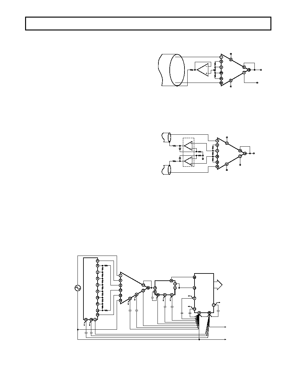
AD625
+VS
–VS
RF
RG
RF
SENSE
REFERENCE
AD711
VOUT
+INPUT
–INPUT
100
Figure 32. Common-Mode Shield Driver
common-mode rejection errors unless the shield is properly
driven. Figures 32 and 33 show active data guards which are
configured to improve ac common-mode rejection by “boot-
strapping” the capacitances of the input cabling, thus minimiz-
ing differential phase shift.
AD625
+VS
–VS
RF
RG
RF
AD712
100
VOUT
SENSE
REFERENCE
–INPUT
+INPUT
–VS
Figure 33. Differential Shield Driver
GROUNDING
In order to isolate low level analog signals from a noisy digital
environment, many data-acquisition components have two or
more ground pins. These grounds must eventually be tied to-
gether at one point. It would be convenient to use a single
ground line, however, current through ground wires and pc runs
of the circuit card can cause hundreds of millivolts of error.
Therefore, separate ground returns should be provided to mini-
mize the current flow from the sensitive points to the system
ground (see Figure 34). Since the AD625 output voltage is
developed with respect to the potential on the reference termi-
nal, it can solve many grounding problems.
AD625
AD7502
–VS
+VS
–VS
+VS
AD583
SAMPLE
AND
HOLD
CAP
–VS
+VS
INPUT
SIGNAL
STATUS
ANALOG
OUT
–VS
+VS
DIGITAL
COMMON
VLOGIC
ANALOG POWER
GROUND
AD574A
A/D
CONVERTER
Figure 34. Basic Grounding Practice for a Data Acquisition System
相关PDF资料 |
PDF描述 |
|---|---|
| TSW-109-05-G-S | CONN HEADER 9POS .100" SGL GOLD |
| AD526ADZ | IC AMP PGA 10MA 16CDIP |
| 53324-0560 | CONN HEADER 2MM 5POS PCB TIN |
| OP470EY | IC OPAMP GP 6MHZ QUAD LN 14CDIP |
| 929836-02-04-RK | CONN HEADER .100 DUAL STR 8POS |
相关代理商/技术参数 |
参数描述 |
|---|---|
| AD625KNZ | 制造商:Analog Devices 功能描述:IC AMP GAIN |
| AD625S | 制造商:AD 制造商全称:Analog Devices 功能描述:Programmable Gain Instrumentation Amplifier |
| AD625SCHIPS | 制造商:AD 制造商全称:Analog Devices 功能描述:Programmable Gain Instrumentation Amplifier |
| AD625SD | 功能描述:IC AMP INST 25MHZ LN 16CDIP RoHS:否 类别:集成电路 (IC) >> Linear - Amplifiers - Instrumentation 系列:- 其它有关文件:TS1854A View All Specifications 标准包装:50 系列:- 放大器类型:通用 电路数:4 输出类型:满摆幅 转换速率:0.25 V/µs 增益带宽积:630kHz -3db带宽:- 电流 - 输入偏压:16nA 电压 - 输入偏移:1000µV 电流 - 电源:162µA 电流 - 输出 / 通道:48mA 电压 - 电源,单路/双路(±):1.8 V ~ 6 V 工作温度:-40°C ~ 125°C 安装类型:表面贴装 封装/外壳:14-SOIC(0.154",3.90mm 宽) 供应商设备封装:14-SO 包装:管件 |
| AD625SD/883 | 制造商:Analog Devices 功能描述: |
发布紧急采购,3分钟左右您将得到回复。